Keywords
|
| ALU, reversible logic, full adder, arithmetic and logic operation, CMOS |
INTRODUCTION
|
| Power is the main issue in present day technology. Reversible logic has received great attention in the recent years due to their ability to reduce the power dissipation which is the main requirement in low power VLSI design. It has wide applications in low power CMOS and Optical information processing, DNA computing. In 1960 R.Landauer’s demonstrated that high technology circuits and systems constructed using irreversible hardware result in energy dissipation due to information loss. A computation is called reversible if its inputs can always be calculated from its outputs. Reversible logic was first related to energy when Landauer [1] states that information loss due to function irreversibility leads to energy dissipation in 1961 who stated that there is a small amount of heat dissipation in the circuit due to the loss of one bit of information and it would be equal to kTln2 where ‘k’ is the Boltzmann constant and T is the temperature. This principle is further supported by Bennett that zero energy dissipation can be achieved only when the circuit contains reversible gates in 1973.It was proved by Bennett [2] that the energy kTln2 would not be dissipated from the circuit if input can be extracted from the output and it would be possible if and only if reversible gates are used. |
| In modern VLSI systems power dissipation is very high due to rapid switching of internal signals. It has been shown that for every bit of information lost in logic computations that are not reversible, kT log2 joules of heat energy are generated. The design that does not result in information loss is called reversible. It naturally takes care of heating generated due to the information loss. Such gates or circuits allow the Reproduction of the inputs from observed outputs and we can determine the inputs from the outputs. Thus reversibility will become an essential property in future circuit design. Reversible logic has applications in various research areas such as low power CMOS design. |
REVERSIBLE LOGIC
|
| A gate is considered to be irreversible if the input and output vectors are not uniquely retrievable. Due to this there will be rapid internal power dissipation. It was proved by Landauer [1] that the computer must dissipate at least KTln2 of energy for each bit of information it writes or erases. Since the number of input vectors cannot be recovered from output vector then information will be lost. |
| In order to overcome the above drawback said by Landauer, Bennet [2] proposed a logic called Reversible logic where the input and output vectors are uniquely retrievable. Reversible gates are circuits in which the number of outputs is equal to the number of inputs and there is one to one correspondence between the input and the output vectors. An example of the reversible gate is shown in fig. It is an n-input n-output logic function in which there is a one-to-one correspondence between the inputs and the outputs. Because of this mapping the input vector can be uniquely determined from the output vector. This prevents the loss of information which is the root cause of power dissipation in irreversible logic circuits. |
| A. FEYNMAN GATE |
| The Feynman gate which is a 2*2 gate and is also called as Controlled NOT and it is widely used for fan-out purposes. The inputs (A, B) and outputs P=A, Q= A xor B. |
| B. FREDKIN GATE |
| Fig. 3 shows a 3*3 Fredkin gate. The input vector is I (A, B, C) and the output vector is O (P, Q, R). The output is defined by P=A, Q=A′B xor AC and R=A′C xor AB. |
| C. PERES GATE |
| Peres gate which is a 3*3 gate having inputs (A, B, C) and outputs P = A; Q = A XOR B ,R = AB XOR C. |
| D. FULL ADDER |
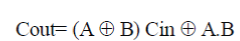
Full adder is the fundamental building block in many computational units. The full adder circuit’s output is given by the following equations: 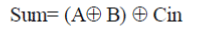 |
 |
| The reversible logic implementation of full-adder circuit and other adder circuits and their Minimization issues have been discussed in [4-7]. It has been shown in previous design that any reversible Logic realization of full adder circuit includes at least two garbage outputs and one constant input. The efficient reversible full adder circuit that is realized using two 3*3 Peres gates only (shown in figure 5). |
RELATED WORK
|
| In [1] Landauer, Rolf. “Irreversibility and Heat Generation in the Computing Process". R Landauer’s showed, amount of heat generation due to loss of bit is kTlog2, and this value is approx 2.8*10-21 joule, which is small but not negligible. The Landauer principle also supported by Bannet. In 1973 Bennet [2] proved that logical reversibility avoid the power consumption in computation. Bennett, Charles H. "Logical Reversibility of Computation". Bennett showed that this heat dissipation due to information loss can be avoided if the circuit is designed using reversible logic gates. No amount of heat would be dissipated from the system as long as the system was able to return to its initial state from its final state. |
| E.Fredkin, T Toffoli, Peres proposed reversible logic gates. Low power combinational circuits design using reversible logic [3] which provides low power consumption. In this paper various logic gates are design with reversibility. Adder circuit is the main module for ALU design.Low power and low cost Adder using reversible logic design we use PERES gate as full adder in which we have low power consumption and low area. |
| The arithmetic and logic unit designing using reversible logic is very important because of low power consumption. The ALU is the main part of any processor for computation. The designing of ALU with reversible logic [9] in this paper reversible ALU design with 22 number of gates and 12 garbage output and more area. This area and number of gate in [8] reduced to 10 which has also more area and more power consumption. The number of gate in [13] reduced to 8 and power consumption is more .The main issue is to reduce the number of gate and also reduced the power consumption. In our design the number of gate reduced to 4 and power consumption is also very low in our proposed design is 1.254 micro watts. |
PROPOSED WORK
|
| In previous ALU design we have more number of gates, transister.constant input, garbage output and more power consumption. In our proposed design the number of gate,transister, constant input, garbage output and power consumption reduced. |
| PROPOSED AIRTHEMATIC UNIT: |
| Airthmetic unit can be design by controlling the one input of adder. In our design we use fredkin gate for controlling one input of the adder. In our design we use Peres gate as full adder shown in fig.6 |
| PROPOSED LOGIC UNIT: |
| In logic unit we perform many logical operations like AND, OR, NAND, NOR, EX-OR. |
| In logic unit we use Peres full adder gate and Feymn gate. |
SIMULATION RESULT
|
| In simulation study we involve the transistor level implementation of arithmetic and logic unit and output waveform of implemented Arithmetic and Logic unit . We simulate our design in TANNER T SPICE TOOL. The simulation of Arithmetic unit is shown in fig.8 . The circuit implementation and simulated output waveform of Logic Unit shown in fig.9 |
| In our simulation result average power consumption is reduced and number of transistor also very less as compared to previous design. Fig.8 show the simulation waveform for arithmetic operation with minimum power consumption ans only two reversible logic gates are used. In fig.9 show the simulated output for logical operations with less power and only two reversible logic gates are used. |
POWER RESULT
|
| The power analysis of previous design and our proposed design shown in fig.10. The power consumption in previous design is more shown in fig.10. In our proposed design we reduced the power consumption which is important in recent research area. We calculate the average power consumption for previous design and our proposed design at various different voltage levels shown in the following power consumption graph. The average power consumption is reduced in our design. |
CONCLUSION
|
| In our proposed design the number of gate ,number of transister, number of constant input are very less as compared to previous design. In our design we have low power and less area which is most important in designing area. In Arithmetic, Logical Unit design we used FREDKIN gate , PERES gate and FEYMAN gate and PFAG. We have compared these proposed design with the existing designs in terms of number of gates used, number of transistor , Garbage outputs, constant inputs, logical & arithmetic functions, and hardware complexity. |
| Proposed design has 4 gate count, 7 garbage output, 1 constant input which are very less in compare to existing design. So the proposed design implementation of ALU in terms of number of gates used, Garbage outputs , number of transistors, constant input can be used for low power applications. In future we can design complete computer architecture with the help of proposed designs. |
Figures at a glance
|
 |
 |
 |
 |
 |
| Figure 1 |
Figure 2 |
Figure 3 |
Figure 4 |
Figure 5 |
|
 |
 |
 |
 |
 |
| Figure 6 |
Figure 7 |
Figure 8 |
Figure 9 |
Figure 10 |
|
References
|
- R. Landauer, “Irreversibility and Heat Generation in the Computational Process”, IBM Journal of Research and Development, 5, pp. 183-191, 1961.
- C.H. Bennett,” Logical Reversibility of Computation”, IBM J .Research and Development, pp. 525-532, Nov. 1973 .
- A. Kamaraj , I. VivekAnand and P. Marichamy ‘’ Design of Low Power Combinational Circuits Using Reversible Logic and Realization in Quantum Cellular Automata’’.IEEE International Conference on Innovations in Engineering andTechnology (ICIET’14) Volume 3, Special Issue 3, March 2014.
- Rao N.S., Aithal S., Haleneer S., Gopal V. ‘’Design of low power adder ‘’.International Journal of Knowledge Engineering ,ISSN: 0976-5816 & E-
- AkashGoel,VineetMonga, Manish Bhalla,ArtiSaxena ’’ Half Adder, Half Subtractor and Full Adder by Using Reversible Gates’’. National Student Conference On “Advances in Electrical & Information Communication Technology”AEICT- 2014
- Hafiz Md. Hassan Babu, Md. Rafiqu Islam, Ahsan Raja Chowdhary and Syed Mostahead Ali Chowdhary “Synthesis of Full Adder circuit using
- Reversible logic”.17th international conference on VLSI Design Mumbai, India, pp 757-760, 2004.
- Bruce, J.W., M.A. Thornton, L. shivakuamaraiah, P.S. kokate and X. Li, “Efficient adder circuits based on a conservative reversible logic gate”, IEEE Computer society Annual symposium on VLSI, Pittsburgh, Pennsylvania, pp: 83-88, 2010.
- Zhijin Guan, Wenjuan Li, Weiping Ding, Yueqin Hang, and Lihui Ni, “An Arithmetic Logic Unit Design Based on Reversible Logic Gates”
- Communications, Computers and Signal Processing (PacRim)v , pp.925-931, 03 October 2011
- Akanksha Dixit, VinodKapse, “Arithmetic & Logic Unit (ALU) Design using Reversible Control Unit” International Journal of Engineering and Innovative Technology (IJEIT) Volume 1, Issue 6, June 2012
- G.V.V.S.R. Krishna ” Behavioral Analysis of Different ALU Architectures” International Journal of Electronics and Computer Science Engineering, 2277-1956/V1N3-1482-1488.
- ArvindRajput , Anil Goyal “Design and Comparison of Low Power & High Speed 4-bit ALU” Proceedings of 2nd National Conference on
- Challenges& Opportunities in Information Technology (COIT-2008) RIMT-IET, MandiGobindgarh. March 29, 2008
- B. Lokesh , K. Dushyanth “ 4 -Bit Reconfigurable ALU with Minimum Power and Delay” International Journal of Computer Applications
- National conference on VSLI and Embedded systems , 0975 – Q8887 ,2013
- ShefaliMamataj ‘’ An Optimized Realization of ALU for 12-Operations by using a Control Unit of reversible gates ‘’. International Journal of
- Advanced Research in Computer Science and Software Engineering Volume 4, Issue 1, January 2014January - 2014, pp. 496-502 .
|