International Journal of Advanced Research in Electrical, Electronics and Instrumentation Engineering
ISSN ONLINE(2278-8875) PRINT (2320-3765)
ISSN ONLINE(2278-8875) PRINT (2320-3765)
M.Ragavan1 and K.Suganthi2
|
| Related article at Pubmed, Scholar Google |
Visit for more related articles at International Journal of Advanced Research in Electrical, Electronics and Instrumentation Engineering
Double Data Rate Dynamic Random Access Memory (DDR DRAM) has become important to develop a low-power high performance DCC(Duty Cycle Corrector) with better duty cycle accuracy. DDR DRAM increases the speed using Successive Approximation Register Duty Cycle Corrector (SAR DCC). The proposed DCC circuit will be implemented in a 0.18- um CMOS process. Here, Adjuster circuit delay line is being modified for low frequency. The main objective of this paper is to achieve fast duty correction . The state-of- the-art DDR DRAM is proposed where a mixed mode DCC. The circuit uses a digital feedback of SAR design process and performance analysis is presented in the paper. The proposed technique will reduce power consumption and speed gets improved in CMOS technology. The entire work can be done by using CADENCE Virtuso
Keywords |
| Double Data Rate(DDR), Duty Cycle Corrector(DCC), Successive Approximation Register(SAR). |
INTRODUCTION |
| For many high-speed systems such as double data rate (DDR) DRAM, double sampling analog-to-digital converter (ADC) and half rate clock data recovery (CDR), bothnegative and positive transition edges of a clock are utilized to double the data rate.In such applications, the clock duty-cycle should be close to 50%. Duty-cycle correctors (DCCs) are widely used to adjust the clock duty-cycle to 50%. Since improving the speed of computer systems demands lowpower high-speed memory such as DDR3 and DDR4 DRAMs.A lot of effort has been devoted to achieve low-power DCCs with better duty-cycle accuracy, wider duty-correction range and short duty-correction time. The non-feedback digital DCCs have the advantage of fast duty-correction and low-power operation.A lot of effort [1]–[10] has been devoted to achieve low-power highperformanceDCCs with better duty-cycle accuracy, wider duty-correctionrange and short duty-correction time. The mixed mode digital feedback using a high speed transition by 7 to 14 cycle. But its needed complex circuit to design to achieve this performance[1]. |
| Conventional DCCs can beclassified into non-feedback and feedback DCCs.The non-feedback digital DCCs [2]–[4] have the advantage of fast duty-correction andlow-power operation. However, the DCCs utilizing interpolation havespeed limitations on the maximum operation frequency [2], [3] and theopen-loop characteristic cannot track the process, voltage and temperature(PVT) variations. In general, it needs complex calibration andtrimming circuitry for compensating PVT variations, which increasesthe area overhead. The analog-feedback DCCs usually adopt the negativefeedback scheme. Since charge pumps [5] or integrators [6] are used to provide the feedback, the analog DCCs can achieve higher dutycycleaccuracy. However, the analog-feedback leads to long duty-correctiontime. Moreover, it requires extremely complex designs to maintainstable operation. In addition, in the DRAM applications with thepowerdown mode, in order to keep the correction information duringthe power-down mode, the DCC control has to be digitally controllable. All digital-feedback DCCs [7], [8] can recover the 50% duty-cyclewithin the very short dutycorrection time. However, DCCs adopt complicatedduty-cycle detector structures such as a time-to-digital converter (TDC)-based detector [7], which increases the cost of hardwareimplementation and the performance of TDC such as the linearity candegrade the entire DCC performance. Other mixed-mode digital-feedback DCCs contain the duty-cycle detector with the simple analog circuits of amplifier [9] or integrator and comparator [10]. However, theseDCCs suffer from long duty-correction time. |
| In this brief, in order to achieve fast duty-correction with small chiparea and low-power consumption, a mixed-mode DCC circuit using adigital-feedback by the successive approximation register (SAR) controllerto support the powerdown mode of the state-of-the-art DDRDRAMs is proposed. This brief is organized as follows. In Section II, the architecture and operation of the general SAR-DCC circuit are describedand Also, the effectiveness of first exploiting the SAR controllerin the DCC circuit is discussed,describes details of the implementedcircuit.. Section III shows the experimental results of the proposedcircuit.Finally, the brief is concluded in Section IV. |
 |
GENERAL SAR - DCC |
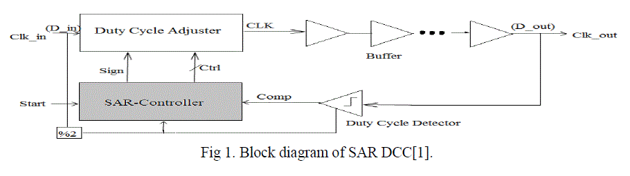
| Fig. 1 shows the block diagram of the proposed SAR-DCC circuit,which consists of a duty-cycle detector, a duty-cycle adjuster, itscontroller and an output buffer[1]. A successive approximation ADC is a type of analog-to-digital converter that converts a continuous analog waveform into a discrete digital representation via a binary search through all possible quantization levels before finally converging upon a digital output for each conversion. The exploited SAR controller, which adopts the binary search algorithm, controls the duty-cycle adjuster to correct the clock duty-cycle by 50%. The duty-cycle detector in this brief just checks whether or not the positive duty-rate DOUT is bigger than 50%. It can be called “a duty-rate comparator”[1]. When the signal Start goes to HIGH, the duty-cycle correction begins with initializing the control signals of the duty-cycle adjuster. All bits of the SAR control word Ctrl are set to LOW. The duty-rate comparingbit Sign of the input clock . CLKIN is determined by the signal Comp, which is the output signal of the duty -cycle detector in the case of no duty-cycle correction of CLKIN[1]. |
| A. Binary Search Algorithm |
| A binary search or half-interval search algorithm finds the position of a specified value within a sorted array. In each step, the algorithm compares the input key value with the key value of the middle element of the array. If the keys match, then a matching element has been found so its index, or position, is returned. Otherwise, if the sought key is less than the middle element's key, then the algorithm repeats its action on the sub-array to the left of the middle element or, if the input key is greater, on the sub-array to the right. If the remaining array to be searched is reduced to zero, then the key cannot be found in the array and a special "Not found" indication is returned. A binary search halves the number of items to check with each iteration, so locating an item (or determining its absence) takes logarithmic time. |
| B.Duty Cycle Detector |
| The duty-cycle detector of the duty-rate comparator comprises an analog amplifier of the logic amplifier, SR latch and inverter buffers . The first folded preamplifier converts the differential clock signals into differential current signals and amplifies the current difference, which is integrated into the capacitors C1 and C2 . |
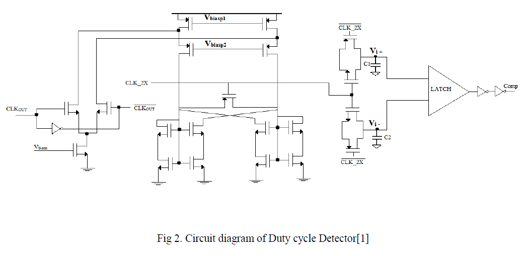 |
| The second differential latch amplifies the integratedvoltage difference to a full swing digital signal. Since the dutyratecomparator operates at high speed, the first stage of the preamplifier requires wide bandwidth. In this work, the first stage is designed withconsideration of the tradeoff between gain and bandwidth. Also, thebias voltages are externally calibrated in order to reduce the mismatch of the integrated current and offset of the latch over the process variation.Fig. 5(b) shows the operation principle of the duty-rate comparator. The comparator in thiswork evaluates and determines the dutyrateat the falling edge of the divided-by-2 clock CLK_2X for the resetphase of the equalization function, which doubles the duty-cycle correctionfrom 7 to 14 cycles[1]. |
| C. Duty Cycle Adjuster |
| The DDR DRAMs require wide operation frequency range with digitally controllable duty-cycle adjuster for the power-down mode. Adopting the phase mixer as a duty-cycle adjuster can achieve better duty-correction resolution. However, it is hard to achieve the wide operation frequency range. In this work, we adopted digitally programmable delay lines the proposed duty-cycle adjuster. The adjuster consists of a variable falling edge generator with 6-bit programmable delay lines [4],[8] and [10] fixed rising edge generator with dummy delay lines, latch, and MUX. The falling edge generator performs the duty-rate adjustment with the non-inverted or inverted signal of the input clock by MUX selection and 6-bit control signals of the programmable delay line[1]. |
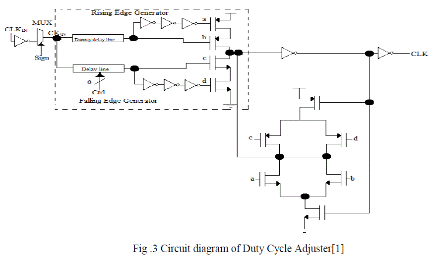 |
| The previous delay-line based duty-cycle adjuster circuits use falling edge generators[10] or both rising and falling edge generators[4],[8] for the duty-rate adjustment. Since a lower frequency operation is also required in DDR DRAM applications, the delay lines of the previous correction circuits are increased. In the case of the conventional dual-edge is used in this circuits, the required minimum amount of the delay line is the period of the lowest operation frequency for the full correction range of 50%. In order to reduce delay lines, we use only a falling edge generator with the input - inversion 2x1 MUX for duty-rateadjustment. While the conventional circuits without the signal inversion require at least 128 delay cells for the required correction range of this work, the length of the delay cells in our adjuster is 64. |
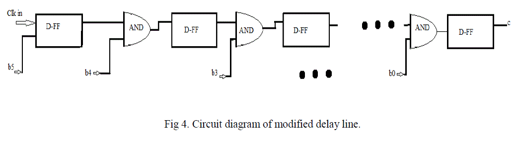 |
| At the first period of the duty-correction, there is no duty-rate change for the Sign determination of the input clock duty-cycle. The Sign lets the non-inverted clock input or the inverted one through as a clock input of duty-cycle adjuster. It cannot guarantee the fixed-delay rising-edge (or falling-edge) clock. However, fig 4. shows the clock input with the selectable edge comparison of the falling edge is comprised in the combination of D-Flip flops and AND gates as a clock generator, the Sign information can be provided to D-flip flop, which can be used as the synchronization information of the delay line. The main drawback of this adjuster may be that the DLL requires a specially designed phase detector that selectively compares the rising and falling edges according to the control signal Sign from the DCC, which results in a complicated DLL design. |
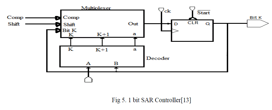
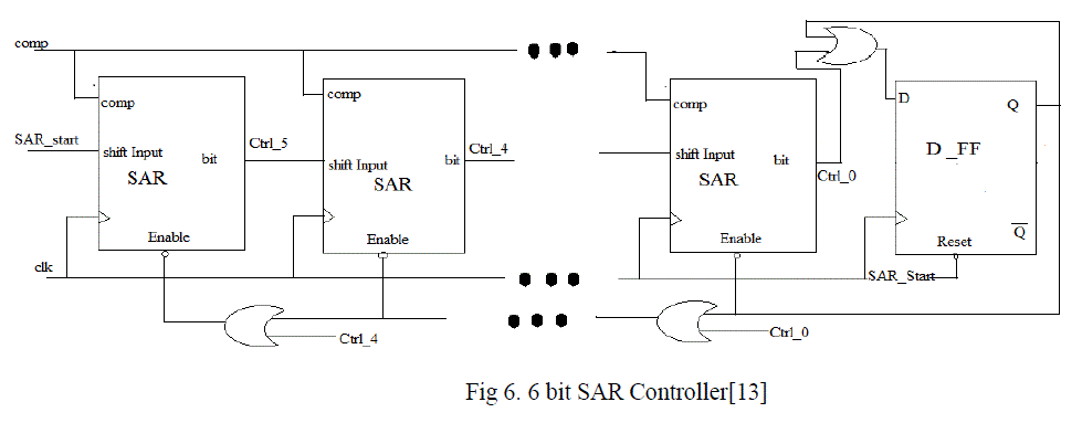
| D. SAR Controller |
| 6-bit SAR block diagram with an additional Signregister, which uses the binary search algorithm for selecting the inputs. The SAR determines the value of each bit of the control word Signand Ctrl according to the sequential binary search based on the outputof the duty-rate comparator Comp. The modified start circuit with the divided-by-2 clock CLK_2X, start signal. After the duty-cycle correction of the LSB determination inthe SAR registers, this SAR circuit gives the information End of thecorrection finish, which goes to HIGH after determining .Thedigitally stored data in SAR can support the power-down mode for theDDR DRAMs. |
 |
 |
| The n-bit control word from the up/down counter determines whether the input clock goes through the delay stage or just passes it. The principle of operation is similar to that case in a RDLL except that the n-bit up/down counter counts up or down to control the delay line. Compared with the RDLL, if 64 delay stages are required in a RDLL, only 6 delay stages are required in a CDLL. Besides, the 64-bit shift register in a RDLL can be replaced by a 6-bit up/down counter. |
EXPERIMENTAL RESULTS |
| CMOS process has been done in cadence at 180 nm with VDD of 1.8v and simulation result is obtained. The total number of transistors is measured which contribute more area and power consumption in the integrated circuit design.The existing adjuster Delay Locked Loop constitutes more transistors which is the complex circuit consuming more power. The proposed adjuster, where in it uses D-flip flops and AND gates thereby reduction in complexity and low power consumption. |
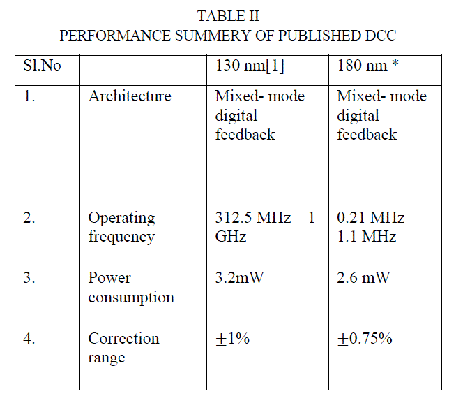
| The performance summary of proposedSAR-DCC is given in Table I, and the performance comparisons withpublished DCCs are also listed. Among the conventional feedback typeDCCs, the all digital-feedback DCC with the large delay lines has the smallest duty-correction time [7]. Comparing with the DCC in [7], theproposed SAR-DCC has the faster duty-correction time as well as occupyinga smaller die area by adopting a simple duty-rate comparator. |
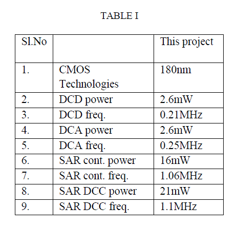 |
| DCD - Duty cycle Detector |
| DCA - Duty cycle Adjuster |
| SAR - Successive Approximation Register |
| SAR DCC - Successive Approximation Register Duty cycle Corrector |
 |
| *This Project |
SIMULATION RESULTS |
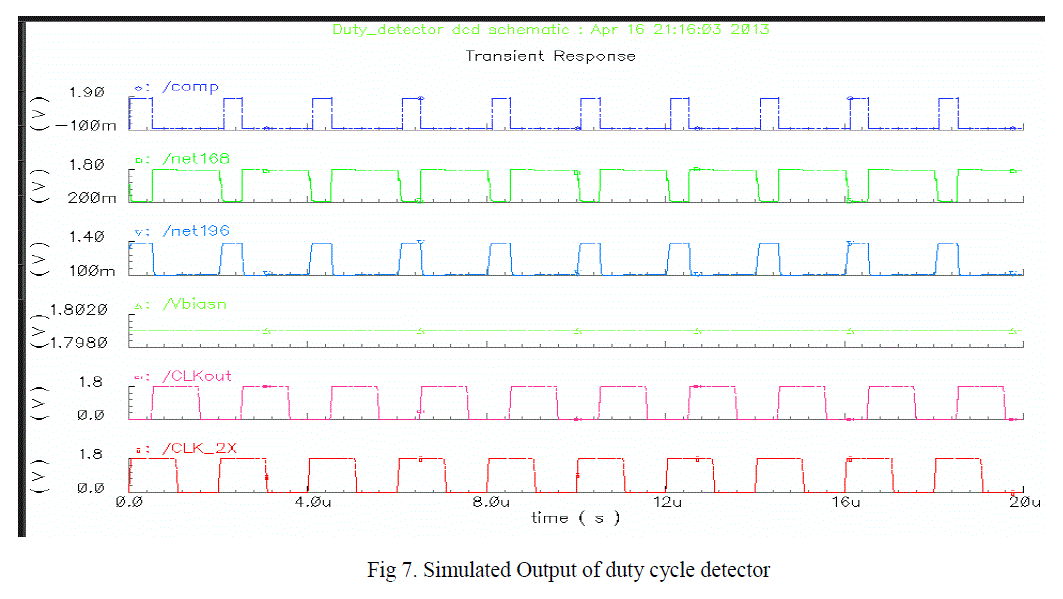 |
| By comparing Clk-out and clk_2x the comparator output which is the input for SAR controller. |
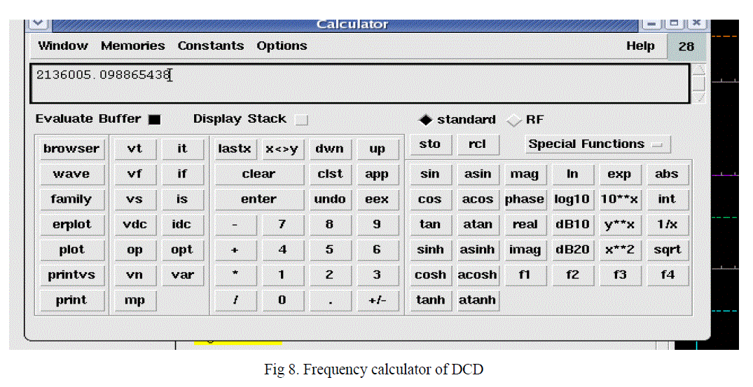 |
| Frequency analysis for duty cycle detector. |
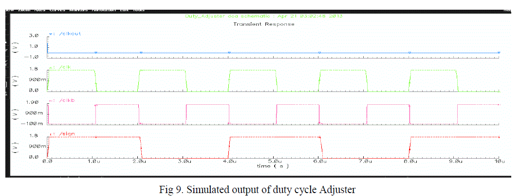 |
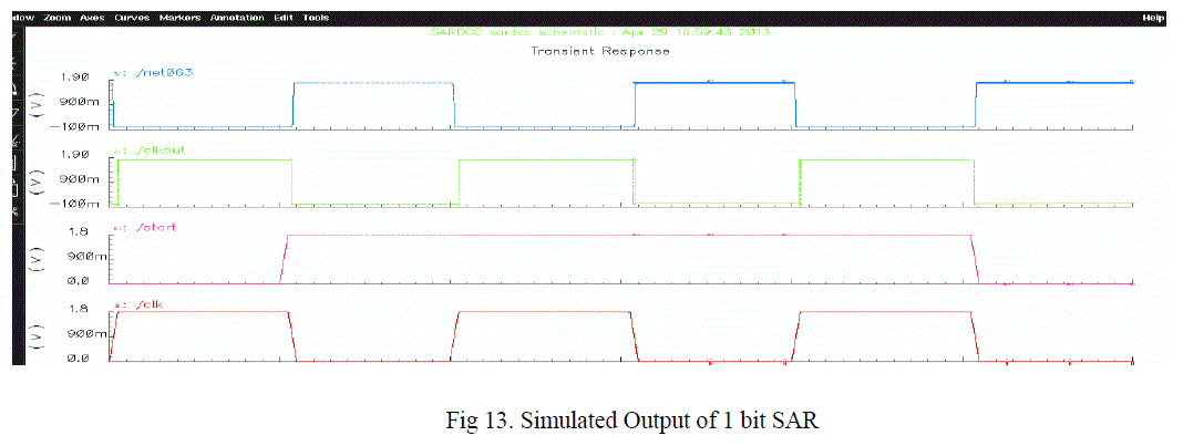
| By giving the clk and sign input to adjust the clk-out. Which is the input of DCD. |
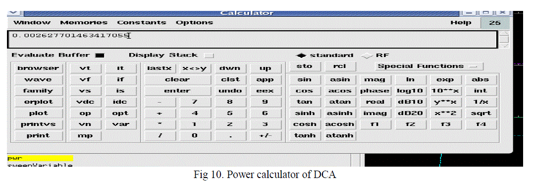 |
| Power analysis of duty cycle adjuster. |
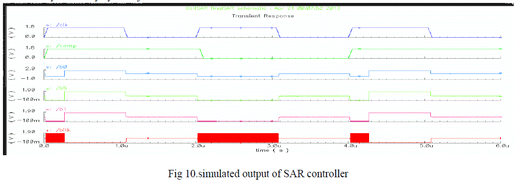 |
| By giving the Comparator clock input to the Duty Cycle Detector and frequency divider, 6 bit binary output and asign bit output is generated as an input to the Duty cycle Adjuster. |
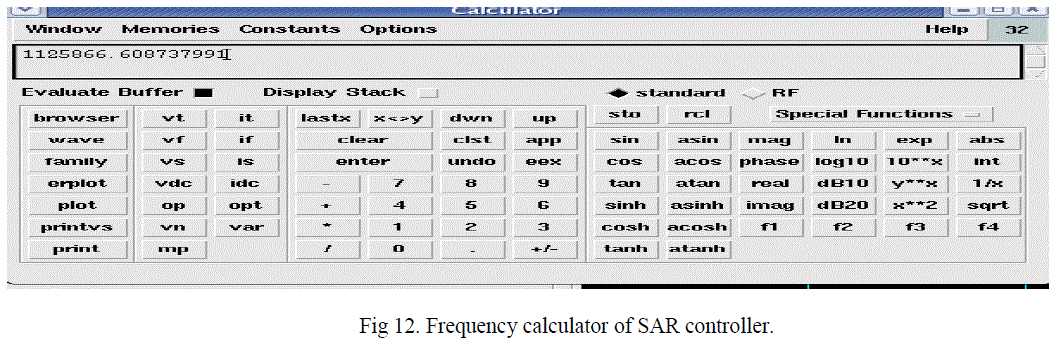 |
| This is the frequency calculator for SAR controller. |
 |
| stored data in SAR can support the power-down mode for theDDR DRAMs. |
CONCLUSION |
| SAR-DCC for DDR DRAM applications is presented. In order to achieve fast duty-correction to support the powerdown mode, a SAR is proposed as a duty-correction controller. Within 7 cycles, the proposed SAR DCC corrects the duty-cycle to 50%,between the frequency range of 0.21MHz to 1.1 MHz and the DCC’s correction range is 40% to 60%, respectively. This proposed SAR-DCC achieves the fastest duty-correction time among feedback type DCCs. Since the duty-cycle adjuster uses delay lines and the duty-cycle detector comprises the differential amplifier, the proposed SAR-DCC may suffer from PVT variations including noises. |
| We have used 180nm technology and result have been tabulated. we have compared our result with 130 nm. In the future this can be implement in 90nm . Because of very low power consumption. Here, adjuster block is modified for low frequency. |
References |
|