International Journal of Advanced Research in Electrical, Electronics and Instrumentation Engineering
ISSN ONLINE(2278-8875) PRINT (2320-3765)
ISSN ONLINE(2278-8875) PRINT (2320-3765)
Ramnik Kour1 and Randeep Singh Chib2
|
| Related article at Pubmed, Scholar Google |
Visit for more related articles at International Journal of Advanced Research in Electrical, Electronics and Instrumentation Engineering
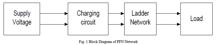
In this paper, a 3-stage type-A pulse forming network have been studied and designed to evaluate the effect of output parameters for different load resistance values. The results are evaluated for different load resistance value while keeping the other components value as static. The reference impedance was set to 50Ω. The high input applied voltage of 1KV is considered for the design and result evaluation purposes. The results are evaluated to see the effect of load current (IZ), capacitor current (IC) and inductor current (IL) for different load resistances.
Keywords |
| Pulse forming network, type A network, ladder network, load current. |
INTRODUCTION |
| The pulsed power is the instant energy released after accumulation for a longer period of time through a switch [1]. The characteristics of this power pulse are based on the load requirement and specification that includes its voltage level and rising time [2]. In the past, pulsed power generators have been generally specified for navigation and nuclear fusion applications [3]. High peak power were used for these purposes whereas moderate peak power are used mainly for industrial applications like food processing, medical and water treatment, ,pulsed high-current linear accelerators, insertion of protein into cell membrane, exhaust gas treatment, gas discharge experiments , engine ignition, and ion implantation [4-9]. |
 |
| Some common technologies that have been utilized for pulsed power supply are Marx Generators (MG), Magnetic Pulse Compressors (MPC), Pulse Forming Network (PFN), Multistage Blumlein Lines (MBL) [10-12]. Several researchers had reported the applications and problems related to PFN and their applications [13]. PFNs consist of the lumped-constant network and are made up of cascaded low-pass LC-filters with non linear phase characteristics. PFN networks generally produce slope waveform at the trailing edge of the output pulse [14]. Since a PFN is an electrical circuit consisting of some switches capacitors, inductors, resistors, and treatment chamber, thus, the shape of a pulse depends on the electric values of each component [15]. Different types of PFN network are being designed that includes Type A, Type B, Type C, Type D, Type E, Type F and Rayleigh line [16]. In this work, Type A ladder network has been studied, analysed and modified to generate pulse waveforms. Further, the value of each component is to be optimized for their applications in high voltage pulse forming networks. |
MATHEMATICAL ANALYSIS |
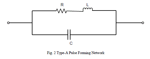
| Type-A network consists of a series combination of resistor and inductor in parallel with a capacitor is shown in fig. 2. |
 |
| The resonant frequency for a single stage Type A network can be evaluated as [17] |
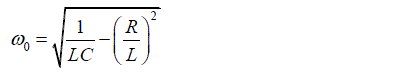 |
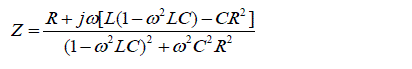
| For such networks, the resonant frequency is that at which the value of admittance is zero for imaginary part. Also the impedance (Z) is given as |
 |
| Its magnitude is found to be |
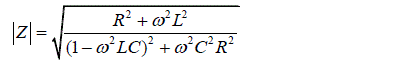 |
| and the phase Angle |
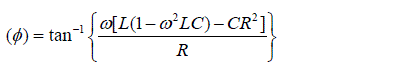 |
| Pulse Width T is given as |
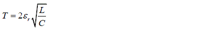 |
| Hence the fundamental components for type-A network are formed by the combination of L’s and C’s. The other elements are used to filter the fundamental shape. |
METHODOLOGY |
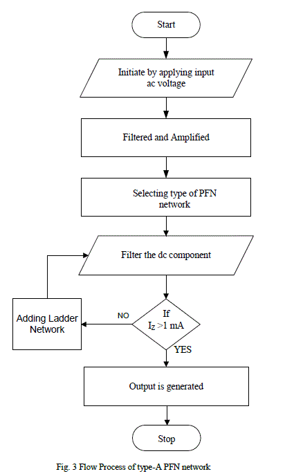
| The design of the type-A PFN network can be explained using the flow chart as shown in fig. 3. The network is initiated by applying high ac voltage of 1KV. The input is then filtered and amplified and is then applied to 3-stage PFN network. The remaining dc component, if any, is again filtered out and the output is generated for the load greater than or equal to 1mA. |
 |
| In this work, the type-A ladder has been studied and simulated for various ladder networks and component parameters. Only 3-stage networks have been simulated for this experiment to know their effect on various output characteristics. Figure 4 shows the n-ladder network for type-A network. |
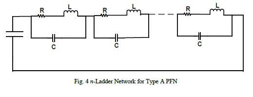 |
| For this type of network, equicells are used. The value of resistances R were selected as 1KΩ while for inductors L and capacitors C, the selected values are 1μH and 1pF respectively. Different load resistances RL were used to evaluate the parametric changes at output. Different loads were taken as 1Ω, 10Ω, 100Ω and 1KΩ. The input voltage applied to the network is 1KV ac voltage with time interval Tint of 50 μs. |
RESULTS AND DISCUSSIONS |
| The results were taken to evaluate the value of load current IL, capacitor current IC and inductor current IL. The experiment was performed in FEM based software MATLAB. Fig. 4 shows the output values for 1Ω load resistance. |
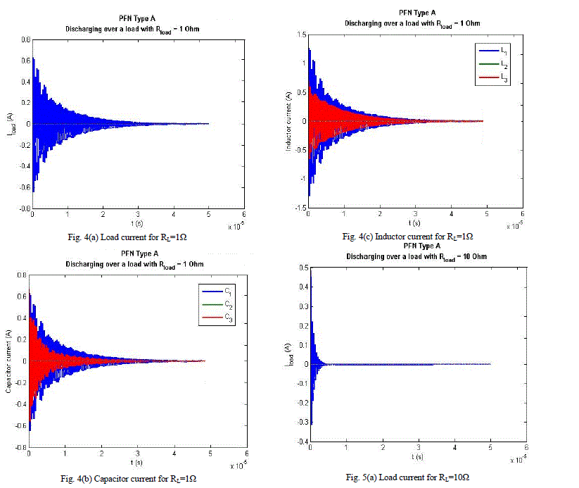 |
| Similarly the results were noted while taken the value of load resistance as 10Ω and is shown in fig. 5. We kept on increasing the load resistance to see its effect on the component parameters. In this regard, the graphs have been noted on the value of load resistance 100Ω as shown in fig. 6. |
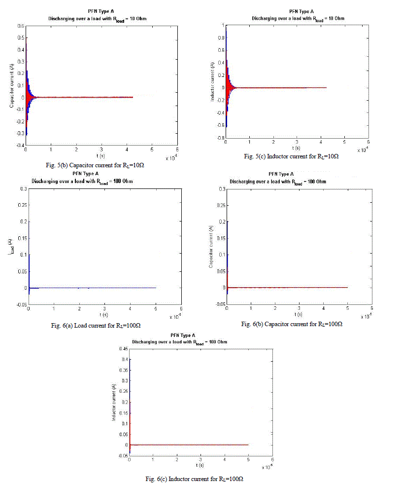 |
| From the plots, it is clear that the frequency response of the network is limited due to inductance in the connections and the energy storage capacitors. Moreover, the response of the circuit would be limited to such an extent that there would be no peak at all. However, the accuracy depends on values of the equivalent circuits with respect to the various components (i.e. series resistance, series inductance, shunt capacitances, etc). Knowing these values, it is a simple circuit calculation to determine the approximate frequency response or the load current of such a circuit built by these passive components, to get the desired waveform in a specific network. |
| The lesser is the value of load, higher is the rise and fall time for the circuit. The slow rise and fall time for across the circuit for higher load value is due to the increased leakage inductance of the circuit. The fundamental component of the waveform can be estimated by the primary capacitance and the series inductance of the circuit. The leakage and loop inductance make up a series inductance which is almost twice the designed value and cannot be changed [18]. The primary capacitance could be lowered to shorten the rise and fall time, but in doing so the peak voltage would drop to an unacceptable level. |
CONCLUSION |
| The design is formed and studied for a 3-stage Type-A PFN network to produce any desired pulse shape. The experiment is done by changing the values of the network components as well as the load resistance. The plots described in the figures show a parabolic rise and fall and ultimately become constant. Moreover, the simulation results show no significant differences in the rise and fall time for different cases, with and without consideration of losses. |
References |
|