Power consumption is an increasing concern in VLSI circuits. To meet the energy requirements new logic circuits have been developed alternatively to standard CMOS. The so-called adiabatic families reduce energy consumption due to the use of a pulsed power supply. A slowly varying voltage source requires less energy to charge a capacitance if its period is longer than the time constant of the charging path and furthermore, when the supply voltage decreases, the output capacitance is discharged and its stored energy can be recovered by the supply source. The goal of this paper is to compare the performances of various adiabatic families with static CMOS and to investigate their robustness against technological parameter variations. The low power dissipation of adiabatic logic families show their importance in green computing. Here the design and analysis are carried out in HSPICE and Tanner SPICE. We have used 180nm technology.
Keywords |
| adiabatic, VLSI, CMOS , SPICE, green computing |
INTRODUCTION |
| The theme for today’s VLSI design and Embedded Systems research is Green Technology - A New Era for Electronics,
which explores the ability of VLSI and embedded circuits and systems to positively impact the environment. Demand for
designing energy-efficient VLSI circuits, improving the efficiency of energy-hungry applications, developing intelligent
monitoring and control systems using integrated circuits or embedded systems to leverage novel green technologies.
Green Technology means the electronic circuits should not hamper our environment. One of the promising technologies
for low power green applications is adiabatic techniques. Power consumption is one of the top concerns of Very Large
Scale Integration (VLSI) circuit design, for which Complementary Metal Oxide Semiconductor (CMOS) is the primary
technology. Today’s focus on low power is not only because of the recent growing demands of mobile & wireless
applications. Even before the mobile era, power consumption has been a fundamental problem. To solve the power
dissipation problem, many researchers have proposed different ideas from the device level to the architectural level and
above. However, there is no universal way to avoid tradeoffs between power, delay and area; designers are required to
choose appropriate techniques that satisfy application and product needs. Power reduction is one of the primary concerns
in VLSI design methodologies because of two main reasons. One is the long battery operating life requirement of mobile
and portable devices and second is due to increasing number of transistors on a single chip leads to high power
dissipation and it can lead to reliability and packaging problems. |
ADIABATIC SWITCHING |
| Power dissipation can be reduced by employing different techniques at different levels of abstraction of the IC design
process. General approaches for reducing power consumption at circuit level are reducing the power supply voltage,
reducing switching activity or reducing load capacitance. Another approach for reducing power dissipation at the
circuit level is usage of AC power supply for recycling energy of node capacitances. The principle is known as
adiabatic which is taken from thermodynamics. In literature, there are two types of adiabatic circuits presented one is
full-adiabatic and other is quasi-adiabatic or partial adiabatic circuits [7]. In adiabatic circuits, energy dissipation can
be separated in two parts. One is an adiabatic loss; the other is a non- adiabatic loss. When a current flow through the
transistor, an adiabatic loss is generated by switching resistance of transistor. That is related with the operating
frequency. In adiabatic charging, the increase of a transition time will make decrease of energy loss. But we can't avoid an adiabatic loss [4, 7]. The non-adiabatic loss occurs due to threshold voltage of transistor. This loss is not related with
operating frequency. It is related to the voltage drop, the node capacitance and the cascading time. Adiabatic switching
which ideally operates as a reversible thermodynamic process, without loss or gain of energy. Adiabatic computation
works by making very small changes in energy levels in circuits sufficiently slow, ideally resulting in no energy
dissipation. There are two types of adiabatic Logic families one is fully adiabatic circuit which is arbitrarily slow. They
lose arbitrarily little energy per operation and almost all of the input energy is recovered in that type of circuit. Another
type of adiabatic logic is partially adiabatic logic or quasi adiabatic logic. Here some amount of energy is recovered and
some energy is lost due to irreversible, non-adiabatic operations [11]. Power loss in conventional CMOS transistors
mainly occurs because of device switching and can be easiest understood by studying the CMOS inverter shown in
Fig.1 |
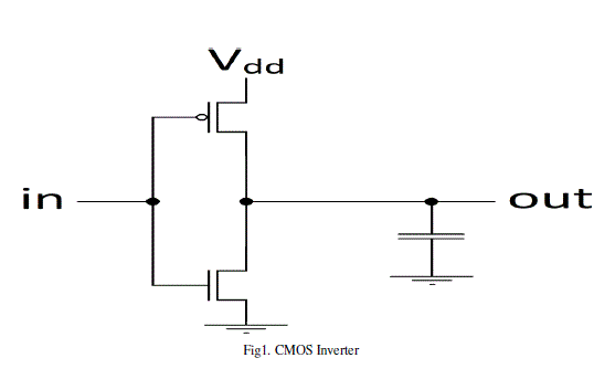 |
| An Inverter consists of pull-up and pull-down transistors connected to a capacitance C. The pull up network pulls the
capacitance output voltage up to Vdd level. The Pull down network pulls down the capacitance voltage 0 from Vdd level.
The capacitance in this case models the fan-out of the output signal. The transistors are in parallel between them and in
serial with C. A more compact way to model this is with an ideal switch and a channel resistance R when in saturation
mode, as shown in Fig. 2. |
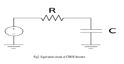 |
| When the logic level is set to high, there is a sudden flow of current from the voltage source, through the ideal switch
and lumped resistor to the capacitance C. The sudden change in voltage level across R accounts for the large amount of
energy lost during CMOS charging. Let us take input voltage =Vdd. When the voltage switches from 0 to Vdd |
| I(t)= Vdd2/R e-t/RC -----------------------------------------------------(1) |
| P(t)= Vdd2/R e-2t/RC --------------------------------------------------(2) |
| E =CVdd2/2 -----------------------------------------(3) |
| In regular CMOS circuits, the energy stored in capacitor is dissipated during discharge cycle on the falling edge of the
clock. Energy stored in capacitor does not need to be minimized, it is necessary to minimize energy wasted in the
transistor network in order to achieve energy savings. |
| If the current is driven with a period T, the total power used in the circuit during a cycle is |
| P=E/T=CVdd22/T---------------------------------------(4) |
| In adiabatic switching ,we use lower frequency and constant current source to minimize power wastage. |
| E=P.Δt=CVdd
2/ Δt. R. Δt ----------------------------(5) |
| If Δt is very long that is infinite, theoretically there will be no energy loss. Infinite charging time is not possible. We
can get constant charging current by replacing constant DC voltage supply with a time varying LC oscillator or driver. |
ADIABATIC INVERTER |
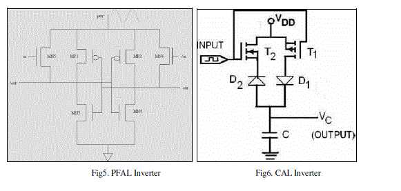
| There are various types of adiabatic inverters. Here we will discuss a few of them. As usual in adiabatic logic circuit
the supply voltage also acts as a clock. Both out and out are generated so that the power clock generator can always
drive a constant Load capacitance independent of input signal. In PFAL, the latch is made by two PMOSFETS and
two NMOSFETS and functional blocks are in parallel with transmission PMOSFET. So, The equivalent resistance
needs to be charged. [4, 5] 2N-2N2P logic reduces coupling effect. The primary advantage of 2N-2N2P over ECRL is
that the cross coupled MOSFET switches result in no floating o/p. Positive Feedback Adiabatic Logic (PFAL) shows
the lowest energy consumption if compared to other similar families .The main part of all the PFAL gates is an
adiabatic amplifier, a latch made by the two PMOS and two NMOS. The two n-trees realize the logic functions. 2N-2N
2P is a modification to ECRL logic. Here the coupling effect is reduced .It has cross coupled latch of two PMOSFET
and two NMOSFET. CAL means cascadable adiabatic logic circuits. This circuit consists of one PMOSFET and a
diode in parallel with one NMOSFET and a diode, which in turn are connected in series with the load capacitance C.
The supply voltage VDD is a slowly varying triangular voltage or a pulsed power supply. The PMOSFET and diode
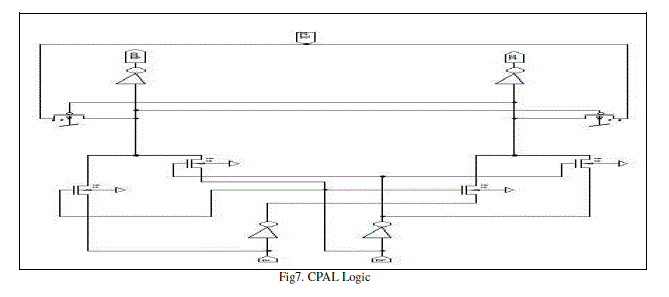
provide a charging path, and the n MOSFET and diode provide a discharging path for the load current. In CPAL
inverting buffers perform restoration of logic levels at the output. Inverting buffers allow driving large capacitive loads.
The PMOS switch performs swing restoration. The PMOS transistors should be properly sized so that the circuit can
function correctly [6]. Here we use ramped power clock as power supply instead of constant DC power supply for less
power dissipation. In DCVSPAL we use complementary outputs so that it is called dual rail logic. The PMOS latch
performs the swing restoration and the time varying ramp is used as power supply instead of constant dc power supply
but due to the floating output there is some amount of power dissipation. |
 |
 |
 |
 |
 |
| |
References |
- N. Weste and K. Eshraghian, Principles of CMOS VLSI Design: A Systems Perspective, 2nd ed. New York: Addison - Wesley,1993.
- M. Pedram, âÃâ¬ÃÅPower minimization in IC design: principles and applications,âÃâ¬Ã ACM Transactions on Design Automation of Electronic Systems,1(1): 3-56,January 1996.
- W. C. Athas, L. J. Svensson, J. G. Koller, et al., âÃâ¬ÃÅLow power digital systems based on adiabatic-switching principles,âÃâ¬Ã IEEE Trans. on VLSI Systems, 2(4): 398-407, December 1994.
- J. S. Denker, âÃâ¬ÃÅA review of adiabatic computing,âÃâ¬Ã in Proc. of the Symposium on Low Power Electronics,1994, pp. 94-97.
- Jan Rabey, MassoudPendram, Low power Design Methodologies:5-7,Kluwer Academic Publishers,5th edition.2002
- P.D. Khandekar, S Subbaraman ,ManishPatil âÃâ¬ÃÅLow power Digital Design Using Energy-Recovery Adiabatic LogicâÃâ¬Ã International Journal of Engineering, Research and Industrial Applications, Vol1, No.III, pp199-2081994, pp. 94-97.
- S.SamantaâÃâ¬ÃÅAdiabatic ComputingâÃâ¬Ã a contemporary reviewâÃâ¬Ã 4th international conference on computer and devices for communication: codec 09.Kolkata .2009.
- S.SamantaâÃâ¬ÃÅ Power Efficient VLSI Inverter Design using Adiabatic Logic and Estimation of Power dissipation using VLSI-EDA ToolâÃâ¬Ã Specialissue of International Journal of computer communication Technology.vol 2.isuue 2,3,4.pp300-303. 2010.
- L.Svensson âÃâ¬ÃÅAdiabatic SwitchingâÃâ¬Ã in low power Digital CMOS Design, Kluwer Academic Publisher, 1995.
- J.Rabacy, Digital Integrated Circuits,PHI,1996.
- Dickinson, A.G. and Denker, J.S., Adiabatic Dynamic Logic, IEEE J. Solid-State Circuits, 1995, vol.30, no. 3,pp.311âÃâ¬Ãâ315.
- V.I Starosel, Adiabatic Logic Circuits: A Review, Russian Microelectronics, 2002, Vol.31, No. 1, pp.37-58.
- Y. Takahashi, Y. Fukuta, T. Sekine, and M. Yokoyama, 2PADCL: Two Phase drive Adiabatic Dynamic CMOS Logic, Proc. IEEE APCCAS,Dec 2006, pp. 1486-1489.
|