In this paper, we have proposed one designs for matrix-matrix multiplication. The one design differs by hardware complexity, throughput rate and different input/output data format to match different application needs. We have compared the proposed designs with the existing similar design and found that, the proposed designs offer higher throughput rate at relatively lower hardware cost. We have synthesized the proposed design and the existing design using Synopsys tools. Synthesis results shows that proposed design on average consumes nearly 30% less energy than the existing design and involves nearly 70% less area-delay-product than other. Interestingly, the proposed parallel-parallel input and single output (PPI-SO) structure consumes 40% less energy than the existing structure.
Keywords |
| Parallel-Parallel Input and Single Output (PPI-SO), Synopsis Simulation. |
INTRODUCTION |
| With the growth in scale of integration, more and more sophisticated signal processing circuits are being
implemented in VLSI chips. These complex signal processing circuits not only demand large computational capacity
but also have high energy and area requirements. Though area and speed of operation remain the major design
concerns, power consumption is also emerging as a critical factor for present VSLI system designers [1]-[4]. The
need for low power VLSI design has two major motivations. First, with increase in operating frequency and
processing capacity per chip, large current have to be delivered and the heat generated due to large power
consumption has to be dissipated by proper cooling techniques, which account for additional system cost. Secondly,
the exploding market of portable electronic appliances demands for complex circuits to be powered by lightweight
batteries with long times between re-charges (for instance [5]. |
| Another major implication of excess power consumption is that it limits integrating more transistors on a single chip
or on a multiple-chip module. Unless power consumption is dramatically reduced, the resulting heat will limit the
feasible packing and performance of VLSI circuits and systems. From the environmental viewpoint, the smaller the
power dissipation of electronic systems, the lower heat pumped into the surrounding, the lower the electricity
consumed and hence, lowers the impact on global environment [6]. |
| Matrix multiplication is commonly used in most signal processing algorithms. It is also a frequently used kernel
operation in a wide variety of graphics, image processing as well as robotic applications. The matrix multiplication
operation involves a large number of multiplication as well as accumulation. Multipliers have large area, longer
latency and consume considerable power compared to adders. Registers, which are required to store the intermediate
product values, are also major power intensive component [7]. These components pose a major challenge for
designing VLSI structures for large-order matrix multipliers with optimized speed and chip-area. However, area,
speed and power are usually conflicting hardware constraints such that improving upon one factor degrades the
other two. |
| With the focus on low power design approach, it was found that much of the progress in the field has been on
component research: better batteries with more power per unit weight and volume; low power CPUs; very low
power radio transceivers; low power displays. Though low-power components and subsystems are essential building
blocks for portable systems, we concentrate on architectural level designing for achieving that goal. A system wide architecture is beneficial because there are dependencies between subsystems, e.g. optimization of one subsystem
may have consequences for the energy consumption of other modules. Therefore, energy reduction techniques have
to be applied in all design levels of the system. Furthermore, as the most effective design decisions are derived from
the architectural and system level, a cautious design at these levels can reduce the power consumption considerably
[8]. |
| We have proposed design for implementing the matrix multiplication operation in hardware keeping the goal of a
power efficient architecture. These designs are verified using various hardware simulating tools.The entire paper has
been partitioned into four parts. In II, proposed architectures for matrix multiplication have been discussed. In III,
hardware complexity and performance comparison of the proposed structure is discussed. In IV, conclusions and
future scope of the paper work has been presented. |
PROPOSED ARCHITECTURE |
| The objective of our paper work was to design efficient low power architecture for matrix multiplication operation.
From the earlier reported works in this field, the major power consuming resource were found to be multipliers and
the registers, used to store and move the intermediate data. So, we have proposed three designs which reduce as well
as optimize the number of multipliers and registers being used in the matrix multiplication operation. For the ease of
recognition we have named the designs on the basis of input and output dataflow. |
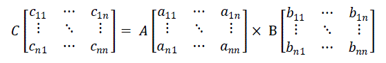
| Let us consider the matrix – matrix multiplication for two n×n matrices A and B given by- |
 (1) (1) |
| Such that, |
 (2) (2) |
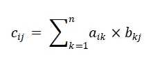
| for all i, j, aik, bkj, and cij represent elements of the n×n matrices A, B and C. |
| • Proposed Parallel-Parallel Input and Single Output(PPI - SO) |
| In this design we have reduced the resource utilization in terms of number of multipliers and registers in lieu of the
completion time. This design is particularly useful where resources are limited and design can be compromised on
basis of increased completion time. The basic working model for a 3 × 3 matrix-matrix multiplication is shown in
Figure 1 below. |
| From equation 2, we observe that each element of the output matrix, C, is computed by multiplying and
accumulating the elements of the corresponding row and column of the input matrices, A and B respectively. This
basic idea is exploited in the design. |
| Considering the matrix – matrix multiplication of two n×n matrices, the calculation is performed using n number of
multipliers, n number of registers and n-1 number of adders. 2 n Cycles are required to perform the matrix
multiplication operation. Each multiplier has two input ports: one each from matrix A and B. In each cycle, n
numbers of multiplications are performed and the products are fed to the adder block to give a single element of the
output matrix, C. The data flow to the multipliers are such that, th k multiplier is fed from th k column of matrix A
and th k row of matrix B, where 1 < k < n. At the th k multiplier, each element from matrix A is repeated for n
consecutive cycles whereas the elements from matrix B are cycled back after n cycles. The partial products are then
fed to the adder which computes the final result. |
| For a better understanding of the process, let us consider the matrix multiplication for n = 3 (as shown in figure 1).
In this case, 3 multipliers and 3 registers are used to calculate and store the partial products respectively. These
partial products are then fed to the adder block to compute the final result. The first multiplier receives input from
the first column of matrix A (ak1) and first row of matrix B (b1k), where. Each element of the matrix A at the first
multiplier is repeated for 3 cycles, such that the data flow can be represented as a11a11 a11 a21a21a21 a31a31
a31.Similarly, at the first multiplier, the elements of B are repeated after 3 cycles, such that the input data-flow will
be b11 b12 b13 b11 b12 b13 b11 b12 b13. The other two multipliers receive the component of A and B in the similar order
as the first multiplier. After the multiplication, the partial products are fed to the adder which computes the elements
of output matrix C in row major order given byc11 c12 c13 c21 c22 c23 c31 c32 c33. So the entire matrix multiplication
operation is performed in
n2=9 cycles. |
SIMULATION RESULT |
| For an×n matrix multiplication, PPI – SO design uses n multipliers and n registers. This design is optimized for
reduced component use and has a penalty of increased operating times (n2 cycles). The input is obtained through 2n
ports and output is calculated out by a single port. This design was compared with prevalent matrix multiplication architecture proposed by Jang et al. [12] to show for the improvements obtained. A comparative theoretical analysis
is given in Table 1. |
| Table 1 shows significant reduction in number of registers used and computation completion time for all proposed
architectures over design of Jang et al [12]. For a better analysis, let us consider the hardware complexities involved
in a 8×8matrix multiplication which forms the basis for DCT computation. DCT matrix can be considered as a
suitable input for all three proposed designs. The aspect ratio of DCT matrix being n = 8 a proper analysis can be
performed for that size. |
| Table 2 shows the Synopsys tools synthesized results for matrix multiplication for matrix size n = 8. The table
shows similar results as obtained for other matrices of size n = 3 to n = 7. PPI – SO provides better throughput rates
and energy requirements. |
CONCLUSION AND FUTURE SCOPE |
| Most of the digital signal processing (DSP) algorithms is formulated as matrix-matrix multiplication, matrix-vector
multiplication and vector-vector (Inner-product and outer-product) form. Few such algorithms are digital filtering,
sinusoidal transforms, wavelet transform etc. The size of matrix multiplication or inner-product computation is usually large for various practical applications. On the other hand, most of these algorithms are currently
implemented in hardware to meet the temporal requirement of real-time application [9]. When large size matrix
multiplication or inner product computation is implemented in hardware, the design is resource intensive. It
consumes large amount of chip area and power. With such a vast application domain, new designs are required to
cater to the constraints of chip area and power and high speed. |
| In this context, we have proposed three designs for power efficient implementation of matrix-matrix multiplication.
The three designs differ by hardware complexity, throughput rate and different input/output data format to match
different application needs. We have compared the proposed designs with the existing similar design and found that,
the proposed designs offer higher throughput rate at relatively lower hardware cost.
As observed through performance comparison, proposed PPI – SO design consumes significantly less energy than
the other proposed design. This is mainly due to the less number of input ports of the design. An energy-efficient
design could be derived by optimizing the number of input and output ports further. |
Tables at a glance |
 |
|
| Table 1 |
Table 2 |
|
| |
Figures at a glance |
 |
| Figure 1 |
|
| |
References |
- T. Arslan, D.H. Horrocks, and A.T. Erdogan,“Overview and Design Directions for Low-Power Circuits and Architectures for Digital SignalProcessing,” IEE Colloquium on Low Power Analog and Digital VLSI: ASICS, Techniques and Applications, pp. 6/1 – 6/5, 1995.
- L. Benini, G. De Micheli, E. Macii, “Designing Low-Power Circuits: Practical Recipes,” IEEE Circuits and Systems Magazine, vol. 1, no.1,pp. 6-25, 2001.
- M. Horowitz, T. Indermaur, R. Gonzalez, “Low Power Digital Design,”IEEE Symposium on Low Power Electronics, pp. 8-11, 1994.
- MassoudPedram, “Design Technologies for Low Power VLSI,” Encyclopedia of Computer Science and Technology, pp. 1 – 32,1995.
- Pramod Kumar Meher, “Hardware-Efficient Systemization of DA-Based Calculation of Finite Digital Convolution,” IEEE Transaction onCircuits and Systems, vol. 53, no. 8, pp. 707 - 711, 2006.
- Pramod Kumar Meher, “New Approach to Look-Up-Table Design and Memory-Based Realization of FIR Digital Filter,” IEEE Transaction on Circuits and Systems, vol. 57, no. 3, pp. 592 - 603, 2010.
- R.B. Urquhart and D. Wood, “Systolic matrix and vector multiplication methods for signal processing,” in IEE ProceedingsFCommunications, Radar and Signal Processing, vol. 131, no. 6,pp.623 – 631,1984.
- S. Tugsinavisut, S. Jirayucharoensak and P. A. Beerelt, “An Asynchronous Pipeline Comparisonswith Applications to DCT Matrix-vectorMultiplication,” in Proceedings of the 2003 International Symposium on Circuits and Systems(ISCAS), vol. 5, pp. V-361 - V-364, 2003.
- J. Lloyd, “Parallel Formulations of Matrix-Vector Multiplication for Matrices with Large Aspect Ratios, ”in IEEE Proceedings of the FourthEuro micro Workshop on Parallel and Distributed Processing, pp. 102-108, 1996.
- O. Mencer, M. Morf, and M. J. Flynn, “ PAM-Blox: High performance FPGA design for adaptive computing,” in Field ProgrammableCustom Computing Machines (FCCM), pp. 167 – 174, 1998.
- Amira, A. Bouridane, and P. Milligan, “Accelerating matrix product on reconfigurable hardware for signal processing,” in Proceedings 11th International Conference on Field-Programmable Logic and Its Applications (FPL), pp. 101 – 111, 2001.
- Ju-Wook Jang, Seonil B. Choi, and Viktor K. Prasanna,” Energy- and Time-Efficient Matrix Multiplication on FPGAs”, IEEE Transaction on Very Large Scale Integration (VLSI) Systems, vol. 13, no. 11, pp. 1305 – 1319, 2005.
|