International Journal of Innovative Research in Computer and Communication Engineering
ISSN ONLINE(2320-9801) PRINT (2320-9798)
ISSN ONLINE(2320-9801) PRINT (2320-9798)
G.Karthikeyan1, Dr.Meena @ jeyanthi2, Ms.S.Soniya3, Ms.Thangaselvi4
|
| Related article at Pubmed, Scholar Google |
Visit for more related articles at International Journal of Innovative Research in Computer and Communication Engineering
A wideband and broad-beam microstrip antenna loaded with gaps and stubs is proposed. The antenna is based on a two-layer stacked electromagnetic coupling microstrip patch antenna (ECMSA). In the analytical cavity model of describing the behavior of MSAs, the antenna is modeled as a cavity with its two side-walls as a perfect magnetic conductor and top- and bottom-walls are perfect electric conductors. Here multiple modes used. Their beams are broader than that of a microstrip antenna with only one excited mode. A conducting cylinder and the coupling aperture are used to excite multiple modes, conducting cylinder connecting the radiation patch and the feed line can influence the parallel connection inductance so that the electromagnetism characters of cavity were changed. Thus antenna most widely used military and commercial applications, its needs to uses antenna size to be reduced but cover the large area. Existing system uses transmission-line model is easy to use, it suffers from numerous disadvantages. It is only useful for patches of rectangular shape, but proposed system meet model expansion analysis. Here the patch is viewed as a thin TMz,-mode, it has cavity with magnetic walls thus uses both rectangular and circular patches, So CRLH structure are more stable than the conducting cylinder. The upper patch of the antenna is loaded with two arc gaps and three stubs in the proposed system. The radiation patch lies on the upper substrate, and the feed line lies between the upper and the lower substrates. Adjusting the size of the two arc gaps and three stubs, changes the operating bandwidth of the exciting multiple modes. The ECMSA is used to achieve wide impedance bandwidth, while the gaps and stubs-loaded patch is used to obtain broad-beam.
Keywords |
| Microstrip patch antenna; bandwidth; beamwidth;radiation pattern; gain; return loss. |
INTRODUCTION |
| Microstrip antennas are becoming increasingly popular since they have small volume and a low-profile planar configuration. Easy mass production of such antennas using printed circuit technology leads to low fabrication cost. They are much easier to be integrated into microwave circuits on the same substrate. Especially, they can be made conformal to the host surface . The above-mentioned advantages make them suitable for numerous applications. The telemetry and communication antenna arrays on missiles are usually microstrip antenna arrays (MAAs). Radio altimeters often use small arrays of microstrip radiators. MAAs have been used for satellite imaging, remote sensing, remote control systems, etc. They have also been used on communication links between ships or buoys and satellites. Smart weapon systems often use MAAs because of their compact configuration and low profile. Moreover, mobile telephones and global positioning systems are major users of microstrip antennas |
| Generally feed technology is used to give supply to the antenna. The following technologies are available: line, probe, proximate, aperture. If two substrate used we can use feeding technique, in case of single substrate port is enough, for power supply. In this proposed system two different substrates are used and the port is used for power supply instead of feeding technique. |
DESIGN OF MICROSTRIP PATCH ANTENNA |
| Microstrip patch antenna feed can be connected directly to the conductor on the same substrate. Many parameters are involved in antenna specification. The most two important parameters in antenna design. Impedance bandwidth: It’s used to radiation and the more power stored in the capacitance and inductance. Pattern bandwidth: The operating frequency of an antenna can be determined by considering the parameters of beamwidth, sidelobe, and gain as minimum or maximum. |
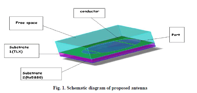
| In the proposed design, two different layer of substrate like Taconic (TLX) and R05880 is used with dielectric constant of 2.2 and 2.55 and thickness of 0.484mm and 1.58mm respectively. The radius of circular radiation patch is 12mm and the port is given to power bottom side of the radiation patch, 50 ohm impedance matching is used for this design. Existing method done only Ansoft HFSS has been used to simulate but now a day Agilent technology to be invented Advance Design System use to design the antenna and easy to analysis the characteristics .Advance Design System (ADS) tool is used to design our proposed antenna for high speed and high frequency platform and also used for easy of analysis. Figure 1 shows the 3D view of microstrip patch antenna. |
 |
SIMULATION RESULTS |
| The dielectric constant of the substrate affects the size of the microstrip antenna. With a higher dielectric constant, the substrate slows the propagating wave through the substrate making the wave slow. Because of this, radiating elements can be smaller. This means the elements are designed at a higher frequency but because of the dielectric constant, the antenna will be operating at a lower frequency. . A disadvantage to patch antenna is the overall efficiency of the antenna. Losses produced by the feed network and the substrate material decrease the overall efficiency. In addition, patch antennas can be susceptible to interference at certain frequencies. Here using two substrate Taconic TLX , Ro5880 with lower dielectric. |
| • Return loss |
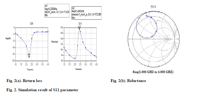
| A trial and error method is used to locate port for measuring the characteristics of S11 parameters of antenna as return loss, reluctance .While designing any antenna we have to consider return loss that should be minimum. In our proposed design return loss is minimized by using port technology. Port is very important in designing multilayer antenna. Using this MSA, RL for the frequency of 2.250GHZ are -17.420db was obtained. Minimum return loss was observed for the design frequency and good reluctance is achieved for our proposed antenna which is shown in the Figure2 (S11 parameter). |
 |
| • Radiation Pattern |
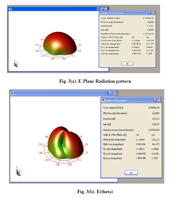
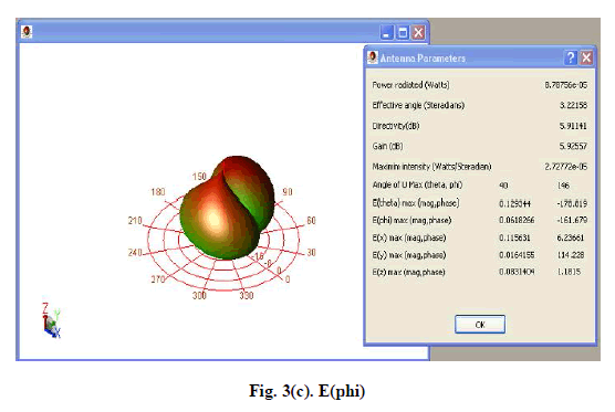
| Radiation of microstrip patch antenna lies on radiation o patch surface. Gain of the radiation pattern in 5.92dB is achieved for the proposed antenna. The magnitude, phase value for E(theta) is 0.1293,-178.819 and E(phi) is 0.0618,- 161.679 respectively. Radiation pattern of the antenna shown in Figure 3. |
 |
 |
CONCLUSION |
| A new way to achieve wider bandwidth and broad beam width of micro strip antennas based on the gap is proposed. The structure of the proposed antenna is based on a two-layer stacked ECMSA. The radiation patch of the ECMSA is loaded with gaps to disturb the surface electric current for the sake of exciting multiple modes. The Gain of radiation pattern in 5.92dB is achieved. The simulation result indicates that the proposed antenna can keep the stable broad beam width and wide bandwidth. |
References |
|