International Journal of Advanced Research in Electrical, Electronics and Instrumentation Engineering
ISSN ONLINE(2278-8875) PRINT (2320-3765)
ISSN ONLINE(2278-8875) PRINT (2320-3765)
Rekhapadman PV1 and Ms.S.Subha2
|
| Related article at Pubmed, Scholar Google |
Visit for more related articles at International Journal of Advanced Research in Electrical, Electronics and Instrumentation Engineering
This paper presents an approach to Embedded Based Flyback Converter with Programmable Switching Frequency for Efficiency Optimization. The fly-back converters are popularly used in digital systems for achieving voltage regulation of dc supply. Normally the switching losses and cost is high in existing system. So here we proposed to develop an embedded based fly-back converter with programmable switching frequency in order to optimize the efficiency. The valley switching technique is used by sensing the valley point of switch voltage with Zero Voltage switching technique. The zero voltage switching technique is used hereto reduce the switching losses.
INTRODUCTION |
| The demands on power supplies for telecom and computer server applications advance with the advancement of information technology. Power- system design for these applications has long been dominated by such issues as efficiency, thermal management, voltage regulation, reliability, power density, and cost. Going forward, these factors will remain critical. |
| A typical breakdown of electricity use and power consumption in data center equipment .It can be observed that computer servers consume more than half of the total energy. Unfortunately, while data centers are booming over the world, the power delivery efficiency for data centers 3 is only around 50%. |
| Flyback converter is the most commonly used SMPS circuit for low output power applications where the output voltage needs to be isolated from the input main supply. The output power of fly-back type SMPS circuits may vary from few watts to less than 100 watts. The overall circuit topology of this converter is considerably simpler than other SMPS circuits. Input to the circuit is generally unregulated dc voltage obtained by rectifying the utility ac voltage followed by a simple capacitor filter. |
| The circuit can offer single or multiple isolated output voltages and can operate over wide range of input voltage variation. In respect of energy-efficiency, fly-back power supplies are inferior to many other SMPS circuits but its simple topology and low cost makes it popular in low output power range. |
CONVENTIONAL FLYBACK DC-DC CONVERTER |
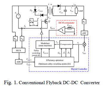 |
| The fly-back converters are popularly used in digital systems for achieving voltage regulation of dc supply. |
| In such fly-back converters usually the dc supply is converted to switched dc using a power switch like MOSFET / IGBT and this high frequency switched dc is coupled to load via a high frequency transformer and rectifier. So the switches will have large power loss. |
| The passive clamp fly back mode has a high turn-off voltage. It is caused by the parasitic oscillation between the transformer leakage inductance and the switch capacitance. The primary switch is traditionally requires the use of a RCD clamp to limit the switch voltage excursion. |
| Unfortunately, in this scheme the energy stored in the transformer leakage is dissipated in the clamp resistor, resulting in a difficult design trade-off between clamping action and clamp circuit power dissipation. |
| Another approach is to replace the diode with a synchronous rectifier, thus reducing the dominant conduction loss in relatively low output voltage applications. However, these modifications come at increased cost. |
LIMITATIONS |
| Disadvantages of this system are Switching losses are high, Cost is high, low efficiency. High turn off voltage and difficult design tradeoff between clamping action and clamp circuit power dissipation. |
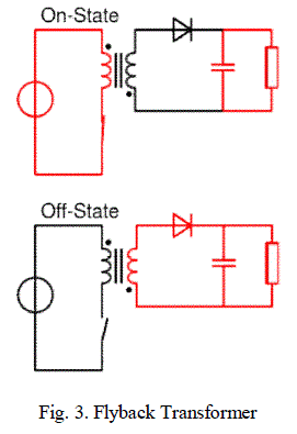
PRINCIPLE OF OPERATION OF FLYBACK DC-DC CONVERTER |
| The flyback converter is used in both AC/DC and DC/DC conversion with galvanic isolation between the input and any outputs. More precisely, the fly back converter is a buck-boost converter with the inductor split to form a transformer, so that the voltage ratios are multiplied with an additional advantage of isolation. When driving for example a plasma lamp or a voltage multiplier the rectifying diode of the buck-boost converter is left out and the device is called a flyback transform. |
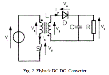 |
| When the switch is closed, the primary of the transformer is directly connected to the input voltage source. The primary current and magnetic flux in the transformer increases, storing energy in the transformer. The voltage induced in the secondary winding is negative, so the diode is reverse-biased the output capacitor supplies energy to the output load. |
| When the switch is opened, the primary current and magnetic flux drops. The secondary voltage is positive, forward-biasing the diode, allowing current to flow from the transformer. The energy from the transformer core recharges the capacitor and supplies the load. |
 |
POWER LOSS MODELING |
| The detailed loss models are necessary in order to per form the efficiency optimization over design and controller parameters. The losses are |
| A Conduction Losses: Conduction losses are modelled on approximate converter waveforms from an ideal-switch converter model. |
| B. Switching Loss Due to Switching-Node Capacitance: At the end of each switching period, the energy stored in the nonlinear switching-node capacitance is dissipated when the switch is turned ON. |
| C. Switching Loss Due to Leakage Inductance: The leakage inductance is analytically modelled from the transformer winding structure and switching loss can be calculated. |
| D. Transformer Proximity Loss and Core Loss: The magneto motive force (MMF) distribution in each transformer winding layer is found in time domain and decomposed into sinusoidal harmonics by Fourier series analysis. The power loss density is then computed for each harmonic, and power loss densities over all harmonics are summed to find the proximity loss in each layer. The core losses are calculated using the improved generalized Steinmetz equation. |
PROPOSED FLYBACK CONVERTER FOR EFFICIENCY OPTIMIZATION |
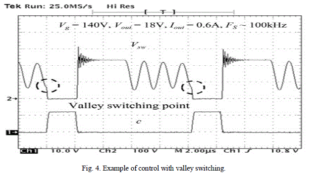
| In this proposed system a novel concept of valley switching is adopted in which ZVS can be provided by sensing the valley point of switch voltage. |
| When the MOSFET switch is turned OFF, there will be oscillations in the switch voltage due to resonance between the magnetizing inductance of transformer and snubber capacitance. |
| The lower most point of these oscillations is called valley point and at this valley point the gate pulse goes high to turn ON the MOSFET in the next cycle. |
| This also helps in zero voltage switching. This technique is called valley switching. Due to zero voltage switching the power loss will be greatly reduced and so the efficiency of the system will be improved. |
| A microcontroller is employed to sense the valley points using ZCD and to generate the PWM pulses for MOSFET switch. The input and output voltage and the input and output current are sensed and fed to ADC of microcontroller to calculate the efficiency. |
| MATLAB Simulator is used to simulate the results. |
 |
| Efficiency optimization in digitally controlled flyback dc-dc converters over wide ranges of operating conditions. Efficiency is characterized and optimized based on power loss modeling and multivariable nonlinear constrained optimization over power-stage and controller parameters. A valley switching technique is adopted to reduce MOSFET turn-on switching loss in discontinuous conduction mode. An optimization procedure is formulated to minimize power loss weighted over a range of operating points, under a cost constraint. A lookup table-based digital controller is applied to achieve on-line efficiency optimization by programming switching frequencies and operating modes based on the efficiency optimization processes. The proposed on-line efficiency optimization approach is verified by experimental results on a low cost 65 W flyback dc-dc prototype. |
SOFTWARE REALIZATION PROPOSED TOPOLOGY OF FLYBACK CONVERTER |
| Input to the circuit may be unregulated dc voltage derived from the utility ac supply after rectification and some filtering. The ripple in dc voltage waveform is generally of low frequency and the overall ripple voltage waveform repeats at twice the ac mains frequency. Since the SMPS circuit is operated at much higher frequency (in the range of 100 kHz) the input voltage, in spite of being unregulated, may be considered to have a constant magnitude during any high frequency cycle. A fast switching device (‘S’), like a MOSFET, is used with fast dynamic control over switch duty ratio (ratio of ON time to switching time-period) to maintain the desired output voltage. |
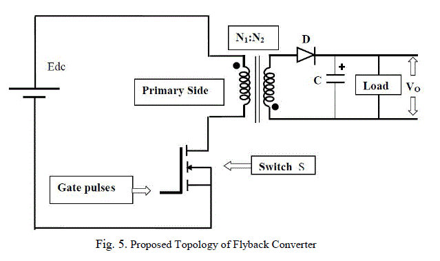 |
| The voltage and current sensing circuit is used to sense the voltage and current. |
| The flyback converter is used in both AC/DC and DC/DC conversion with galvanic isolation between the input and any outputs The voltage clamp is used by electro physiologists to measure the ion currents across the membrane of excitable cells, such as neurons, while holding the membrane voltage at a set level. Electrophysiology is the study of the electrical properties of biological cells and tissues The voltage clamping diode is used for voltage limitation and freewheeling diode is used for prevent the flow of reverse current in this circuit. |
| A fast switching device, like a MOSFET, is used with fast dynamic control over switch duty ratio (ratio of ON time to switching timeperiod) to maintain the desired output voltage. A transformer is a power converter that transfers electrical energy from one circuit to another through inductively coupled conductors— the transformer's coils The transformer is used for voltage isolation as well as for better matching between input and output voltage and current requirements. The secondary winding voltage is rectified and filtered using just a diode and a capacitor. Voltage across this filter capacitor is output voltage. |
| A flyback diode is a diode used to eliminate flyback, the sudden voltage spike seen across an inductive load when its supply voltage is suddenly reduced or removed. A rectifier is an electrical device that converts alternating current (AC), which periodically reverses direction, to direct current (DC), which flows in only one direction Zero crossing detectors as a group are not a well-understood application, although they are essential elements in a wide range of products In simulation, the output is connected to R-Load and it is viewed through the scope. |
EFFICIENCY OPTIMIZATION OF FLYBACK CONVERTER |
| Efficiency optimization in digitally controlled flyback dc-dc converters over wide ranges of operating conditions. Efficiency is characterized and optimized based on power loss modeling and multivariable nonlinear constrained optimization over power-stage and controller parameters. A valley switching technique is adopted to reduce MOSFET turn-on switching loss in discontinuous conduction mode. An optimization procedure is formulated to minimize power loss weighted over a range of operating points, under a cost constraint. A lookup table-based digital controller is applied to achieve on-line efficiency optimization by programming switching frequencies and operating modes based on the efficiency optimization processes. The proposed on-line efficiency optimization approach is verified by experimental results on a low cost 65 W flyback dc-dc prototype. |
| A flyback converter design requires many tradeoffs and iterations with a large number of design variables. The first step of the optimization procedure is to determine the external specifications of the converter (e.g., range of operating conditions,Vg,i and Iout,j ) and component limits used as constraints in the optimization. The core size, core material, output capacitor, and output diode are defined as the constraints in this optimization, and are kept the same as in the power stage prototype used for the loss model.Other constraints are defined for the selection of wires in the transformer, magnetizing inductance, and the clamp voltage Vclamp in the snubber. Round wires are used for transformer windings and a window area is filled such that copper losses due to the DC resistances are minimized.]. The magnetizing inductance is determined for the core not to be saturated using |
| LM IQ,peak < N1BmaxAC |
| where N1 is the number of turns on the primary side, Bmax is the maximum flux density, and AC is the cross-sectional area of the given core. The maximum possible clamp voltage Vclamp is selected based on the voltage rating of the selected MOSFET to minimize the leakage inductance loss. The interleaved transformer is employed in the optimization process because the leakage inductance can be significantly reduced compared to the noninterleaved transformer .Furthermore, it is assumed that the controller employs valley switching at all DCM operating points. |
EFFICIENCY OPTIMIZATION IN OUT |
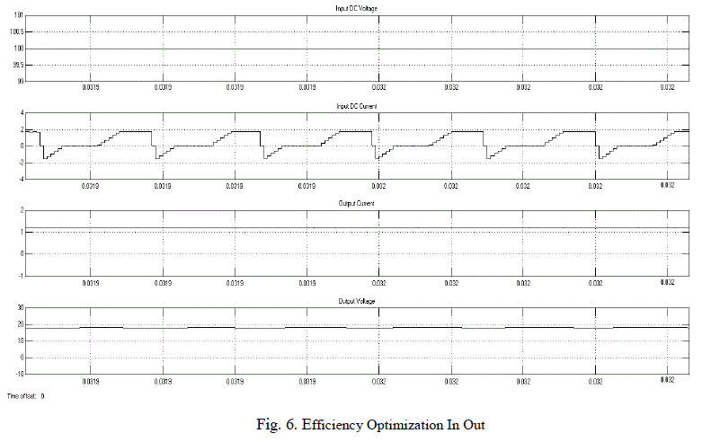 |
EFFICIENCY OPTIMIZATION OF MOSFET |
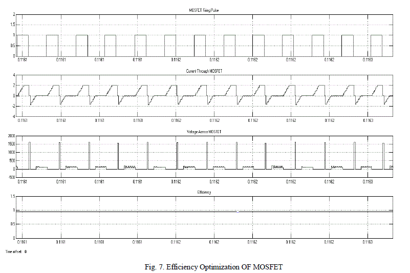 |
| The input and output voltage is measured by the voltage measured block. The pulse generator is used to triggering the mosfet and the mosfet pulse is measured by voltage measurement block. The current is measured by the current measurement block in the primary side of the transformer. The product of input voltage and current is given to the divide block and also the product of output voltage and current is given to the divide block. Then the input and output power is compared using divide block. Finally the efficiency is calculated. |
| In this systems switching losses are reduced,. Low cost compared to existing system. High efficiency. Reduced turn off voltage. These are used in low-power switch-mode power supplies,Power conversion applications.In this systems closed loop control can be employed by sensing the load voltage and fed to ADC of microcontroller. Then the load voltage can be compared with a set value and the error signal can be used to modify the duty ratio of power switch using pid/fuzzy logic to achieve the desired load voltage |
CONCLUSION |
| Efficiency optimization is an approach for digitally controlled flyback dc–dc converters. Efficiency is characterized and optimized over wide ranges of operating conditions based on detailed power loss models and multivariable nonlinear constrained optimization. The proposed efficiency optimization approach can be separated into two processes, the design parameter optimization and the controller parameter optimization, enabling the power stage design and the controller design simultaneously, under a low-cost constraint. The optimum controller parameters are programmed in the lookup table, which implies that the same controller could be applied to different power stages. Compared to other on-line efficiency optimization techniques, the approach is simpler and less susceptible to disturbances during converter operation. Undesirable frequency hopping mechanisms, commonly observed in valley switching control schemes, are resolved by storing optimum valley switching points in the lookup table and by using hysteresis bands in the lookup table boundaries. A gain-scheduled compensator is designed based on small-signal modeling and analysis, and a simple extension, referred to as control, is proposed to improve large-signal transient responses. |
References |
|