Keywords
|
| Space vector pulse width modulation, nine-switch converter, power conditioner, and power quality. |
INTRODUCTION
|
| Static power converter development has grown rapidly with many converter topologies now readily found in open literature. Accompanying this development is the equally rapid identification of application areas, where power converters can contribute positively toward raising the overall system quality [1]. In most cases, the identified applications would require the power converters to be connected in series or shunt, depending on the operating scenarios under consideration. In addition, they need to be programmed with voltage, current, and/or power regulation schemes, so that they can smoothly compensate for harmonics, reactive power flow, unbalance, and voltage variations. For even more stringent regulation of supply quality, both shunt and series converter are added with one of them tasked to perform voltage regulation, while the other performs current regulation. Almost always, these two converters are connected in a back- to-back configuration [2], using 12 switches in total and sharing a common DC-link capacitor, as shown in Fig. 1. A micro source can also be inserted to the common DC link. |
| This paper proposes a single stage integrated nine-switch power conditioner, presenting a better reduced semiconductor alternative for high quality series–shunt compensation, whose circuit configuration is shown in Fig. 2. The proposed conditioner uses a nine-switch converter with two sets of output terminals, instead of the usual 12 switch back-to back converter. The nine-switch converter was earlier proposed in [7], [8] at about the same time, and was recommended for dual motor drives [9], rectifier–inverter systems, and uninterruptible power supplies [10]. Despite functioning as intended, these applications are burdened by the limited phase shift and strict amplitude sharing enforced between the two terminal sets of the nine-switch converter. More importantly, a much larger DC-link capacitance and voltage need to be maintained, in order to produce the same ac voltage amplitudes as for the back-to-back converter. The larger DClink voltage would overstress the semiconductor switches unnecessarily, and might to some extent overshadow the saving of three semiconductor switches made possible by the nine-switch topology. |
OPERATING PRINCIPLES OF NINE SWITCH POWER CONDITIONER
|
| The proposed converter has three legs with three switches per leg. The novelty of this converter is that the middle switch in each of the converter legs is shared by the rectifier and inverter, thereby reducing the switch count by 33% in comparison to the back-to-back converter. The utility power is delivered to the load partially through the middle switches (direct AC/AC conversion) and partially through a quasi DC link circuit. |
| A. Back-to-Back Converter Limitations and Recommendation |
| Fig. 1 show the per-phase representation of the common back-to-back unified power quality conditioner (UPQC), where a shunt converter is connected in parallel at the point-of- common-coupling (PCC), and a series converter is connected in series with the distribution feeder through an isolation transformer. The shunt converter is usually controlled to compensate for load harmonics, reactive power flow, and unbalance, so that a sinusoidal fundamental current is always drawn from the utility grid, regardless of the nonlinearity of load. The series converter is controlled to block grid harmonics, so that a set of three phase fundamental voltages always appears across the load terminals [13]. |
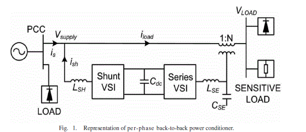 |
| The back-to-back UPQC is still complex and quite underutilized, even though it offers independent control of two decoupled converters. Its underutilization is mainly attributed to the series converter, whose output voltages are usually small, since only small amount of grid harmonics need to be compensated by it under normal steady-state conditions, especially for strong grids(VSUPPLY ≈ VLOAD ). During sag, the converter is sized to inject a series voltage of 1.15 p.u., then the converter modulation ratio is low such as 0.05 × 1.15 [12] with triplen offset included [13]. |
| B. The Nine Switch Converter Operating Principles and Existing Constraints |
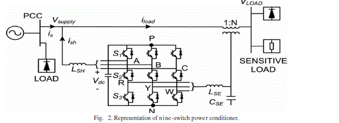 |
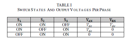
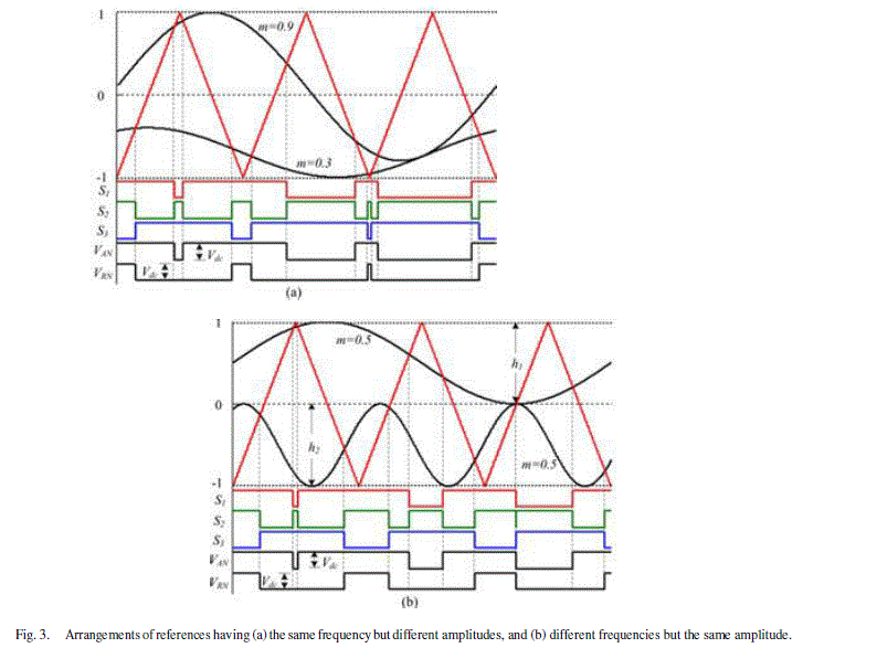
| Fig. 2 shows the nine-switch converter formed by using three semiconductor switches per phase, giving a total of nine for all three phases. The nine switches are powered by a common DC link capacitor. The nine-switch converter faces limitations imposed on its assumable switching states, unlike the fully decoupled back-to-back converter that uses 12 switches. The allowable switching states are shown in Table I, from which, it is clear that the nine-switch converter can only connect its two output terminals per phase to either Vdc or 0 V, or its upper terminal to the upper DC rail P and lower terminal to the lower DC rail N. The last combination of connecting its upper terminal to N and lower terminal to P is not realizable, hence constituting the first limitation faced by the nine-switch converter. Imposing this basic rule of thumb on reference placement, then results in those gating signals drawn in Fig. 3 for the three switches S1, S2 and S3 per phase. Equations for producing the gating signals can be stated as |
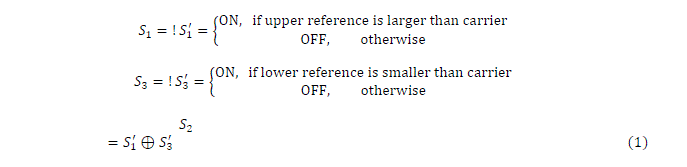 |
| Where is XOR operator? Signals obtained from eqn. (1), when applied to the nine-switch converter, then output voltage transitional diagrams drawn in Fig. 3 for representing VAN and VRN per phase are obtained. Together, these voltage transitions show that the forbidden state of = 0V and is effectively blocked off. The blocking is, however, attained at the incurrence of additional constraints limiting the reference amplitudes and phase shift. These limitations are especially prominent for references having sizable amplitudes and/or different frequencies, as exemplified by the illustrative cases shown in Fig. 3(a) and (b). |
 |
 |
| C. Proposed Nine-Switch Power Conditioner |
| Under normal operating conditions, the output voltage amplitude of the shunt converter is comparatively much larger than the voltage drop introduced by the series converter along the distribution feeder. That means the modulating reference needed by the shunt converter is much larger than the series converter, which simply consist of inverse harmonic components for grid voltage compensating purposes. Drawing these details in the carrier range would then result in a much wider vertical range h1 in diagram of Fig. 3 for controlling the upper shunt terminal, and a narrower for controlling the lower series terminal ( If can be set to zero, if an ideal grid with no distortion and rated sinusoidal voltage is considered. In that case, the lowest three switches, labeled as S3 for each phase in Fig. 2, should always be kept ON to short out the series coupling transformer, and to avoid unnecessary switching losses. |
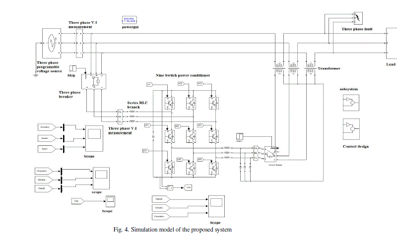
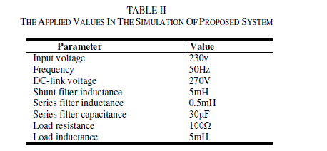
| The and carrier band divisions shown in the Fig. 3, it will need a higher DC-link voltage. The modulation ratio of the series converter can be as low as 0.05 × 1.15 with triplen offset included, the increase in DC-link voltage is merely about 5%, the same maximum shunt voltage amplitude can be produced by the nine-switch converter. This maximum is arrived at a reduced maximum modulation ratio of 0.95 × 1.15, instead of 1.15 with triplen offset considered. The nineswitch converter can be confirmed as a favorable topology for the “series–shunt” power conditioner, is to study its compensating ability under voltage sag condition. For that purpose, the PCC voltage in Fig. 2 is assumed to dip by some amount, which would then subject the higher shunt terminal of the nine-switch converter to a reduced voltage level. In contrast, the lower series terminal must respond immediately by injecting a sizable series voltage at the fundamental frequency ( where is the demanded load voltage reference), so as to keep the load voltage close to its pre fault value. Fig. 4 shows the MATLAB/SIMULINK model of the proposed Integrated nine switch power conditioner. Table II shows the applied parameters in the simulation of proposed system. |
 |
 |
CONTROL STRATEGY
|
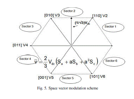
| The control strategy of proposed nine- switch UPQC includes optimal space vector (SV) modulation scheme. Two independent three-phase SV modulators are used to control two machines. References for each machine become vectors in the respective d-q planes, each with a completely arbitrary position, situated in any of the six sectors in their planes. Assuming that both modulators operate in the standard manner (in continuous modulation) where total time of application of zero SVs is equally shared among zero SVs 000 and 111, each reference SV will be realized on average over the switching period by means of two adjacent active SVs. Outputs, generated from the three-phase SV modulators, can be considered as duty cycle values d over the switching period for each of the three legs. In a similar way as with the carrier-based PWM, a simple summing of the duty cycles generated from each modulator can be used to determine the resulting duty cycles of the nine switches UPQC shown in Fig 5. The nine-switch converter only allows upper DC-rail clamping for its upper terminals, and lower DC-rail clamping for its lower terminals, which so far can only be met by the less commonly adopted 120° discontinuous modulation scheme. |
 |
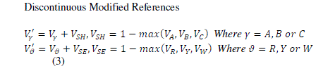
| Discontinuous Modified References |
 |
 |
| Where { MSH, ωSH, θSH} a r e the modulation ratio, angular frequency, and initial phase of the shunt terminals, and { MSE, ωSE, θSE} are the corresponding quantities for the series terminals. Using eq. (2), (3), the modulation plots show the upper reference tied to only the upper DC-rail and lower reference tied to only the lower DC-rail for a continuous duration of 120âÃâæ per fundamental cycle. The 120 discontinuous scheme is indeed a suitable scheme for reducing its commutation count by 33%. Lower commutation count would then lead to lower switching losses, whose values depend on the current amplitudes and phases at the two terminals per phase, like all other converters modulated discontinuously. |
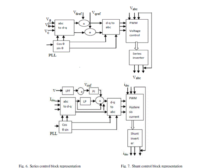 |
| The series terminals of the nine-switch UPQC are given two control functions that can raise the quality of power supplied to the load under normal and sag operating conditions. The series terminals of the conditioner are used to compensate for any harmonic distortions that might have originated at the PCC. They also help to regulate the load voltage to compensate for any slight fundamental voltage variation. |
| The second functionality is, under voltage sag condition. Where a sizable series voltage needs to be injected to keep the load voltage nearly constant. The overall block diagram realized is shown in Fig. 6. The computed voltage error is then fed through a PI regulator in the synchronous frame, whose effect is to force the steadystate error to zero, and hence compensating for those unaccounted voltage drops appearing across the inductive elements. Note that for the control presented here, the synchronous frame is chosen simply because the load voltage reference can then be represented by a single DC constant. If frame transformation is not preferred, resonant regulator in the stationary frame can be used instead, so long as three-phase sinusoids are also used as the load voltage references |
| B. Shunt Control Principles |
| The shunt terminals of the nine-switch power conditioner are programmed to compensate for downstream load current harmonics, reactive power, and to balance its shared DC-link capacitive voltage. To realize these control objectives, an appropriate control scheme is drawn in Fig. 7, where the measured load current is first fed through a high-pass filter in the synchronous frame. The filter blocks fundamental d-axis active component, and passes forward the harmonics and q-axis reactive component for further processing. In parallel, a PI regulator is also added to act on the DC-link voltage error, forcing it to zero by generating a small d-axis control reference for compensating losses, and hence maintaining the DC-link voltage constant. The sum of outputs from the filter and PI regulator then forms the control reference for the measured shunt current to track. Upon tracked properly, the source current would be sinusoidal, and the load harmonics and reactive power would be solely taken care of by the proposed power conditioner. |
SIMULATION RESULTS
|
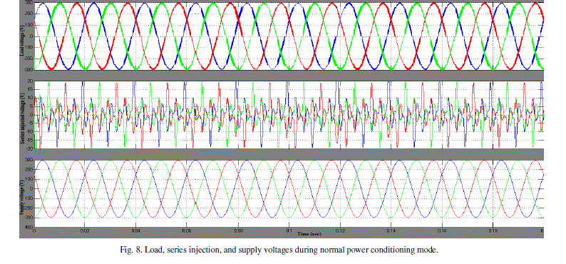
| The performance of the proposed integrated nine switch power conditioner is evaluated with a detailed simulation model using MATLAB/SIMULINK. Fig. 8 shows the supply voltage, series injection voltage and load voltage with a higher grid THD, and with both series and shunt compensation activated. The supply voltage is distorted and appears across the load if series compensation is deactivated and the transformer is bypassed. With the injection of series voltage the source voltage become sinusoidal and having fewer harmonic. |
 |
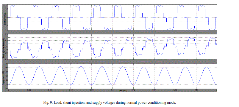
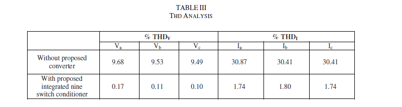
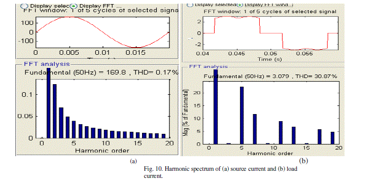
| Fig. 9 shows the load, shunt injection and supply currents conditioned by the nine switches UPQC to verify its shunt compensating capability. The load current is heavily distorted due to nonlinear diode rectifier load, but the source current approached sinusoidal due to the compensation current injected by shunt compensator. The THD in source current is 0.17% and in load current of phase A it is 30.07% from the harmonic spectra shown in Figs.10.Thus the proposed nine-switch UPQC is effective in smoothing the load voltage and load current regardless of the extent of low order grid harmonic distortion introduced and the results are shown in Table III. |
 |
 |
 |
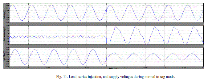
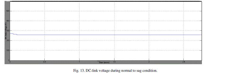
| A programmable source is used to introduce sag. Fig. 11 shows the compensated load voltage, series injection voltage, sagged grid voltage during normal to sag condition. The grid voltage is sinusoidal throughout the whole transitional process with decrease in amplitude during sag period. This decrease in grid voltage is transferred to the series terminal of the nine switch power conditioner. The decrease in power is associated with low series voltage is forced out to shunt terminal, need to maintain load voltage unchanged. Fig. 12 shows the compensated load current , shunt injection current, grid current during normal to sag condition. The DC-link voltage of nine switch power conditioner is always to maintain higher than the back to back conditioner. Fig.13 shows the conditioner DC-link voltage regulated at 270V throughout the whole sag transition. |
 |
 |
 |
CONCLUSION
|
| The nine switch converter based UPQC is simulated using MAT LAB/SIMULINK. It effectively reduces the current and voltage harmonics. The nine-switch converter is more suitable for replacing back- to-back converter in “series– shunt” systems. As a further performance booster, a modified space vector modulation and 120 degree modulation scheme is presented for reducing the overall commutation count by 33%. It is also compensated for voltage sags, total harmonic distortion with proper series and shunt controls. Since the number of switches required is less compared to conventional converter, the switching losses are less. |
References
|
- B. Han, B. Bae, H. Kim, and S. Baek, “Combined operation of unified power-quality conditioner with distributed generation,” IEEE Trans. Power Delivery, vol. 21, no. 1, pp. 330–338, Jan. 2006.
- V. Khadkikar and A. Chandra, “A new control philosophy for a unified power quality conditioner (UPQC) to coordinate load-reactive power demand between shunt and series inverters,” IEEE Trans. Power Del., vol. 23, no. 4, pp. 2522–2534, Oct. 2008.
- Y. , W. Li, D. M. Vilathgamuwa, and P. C. Loh, “A grid-interfacing power quality compensator for three-phase three-wire micro grid applications,” IEEE Trans. Power Electron., vol. 21, no. 4, pp. 1021–1031, Jul. 2006.
- P. C. Loh, F. Blaabjerg, F. Gao, A. Baby, and D. A. C. Tan, “Pulse width modulation of neutral-point-clamped indirect matrix converter,” IEEE Trans. Ind. Applicant., vol. 44, no. 6, pp. 1805–1814, Nov./Dec. 2008.
- E. Ledezma, B. McGrath, A. Munoz, and T. A. Lipo, “Dual ac-drive system with a reduced switch count,” IEEE Trans. Ind. Applicat., vol. 37, no. 5, pp. 1325–1333, Sep./Oct. 2001.
- M. Jones, S. N. Vukosavic, D. Dujic, E. Levi, and P. Wright, “Five-leg inverter PWM technique for reduced switch count two-motor constant power applications,” IET Proc. Electric Power Applicat., vol. 2, no. 5, pp. 275–287, Sep. 2008.
- C. Liu, B. Wu, N. R. Zargari, D. Xu, and J. Wang, “A novel three- phase three-leg ac/ac converter using nine IGBTs,” IEEE Trans. Power Electron., vol. 24, no. 5, pp. 1151–1160, May 2009.
- T. Kominami and Y. Fujimoto, “A novel three-phase inverter for indepen- dent control of two three-phase loads,” in Proc. IEEE-Ind. Applicat. Soc. (IAS)s, 2007, pp. 2346–2350.
- T. Kominami and Y. Fujimoto, “Inverter with reduced switching-device count for independent ac motor control,” in Proc. IEEE-IECON, 2007, pp. 1559–1564.
- C. Liu, B. Wu, N. R. Zargari, and D. Xu, “A novel nine-switch PWM rectifier-inverter topology for three-phase UPS applications,” in Proc. IEEE-Everyday Practical Electron. (EPE), 2007, pp. 1–10.
- S. M. Dehghan, M. Mohamadian, and A. Yazdian, “Hybrid electric vehiclebased on bidirectional Z-source nine-switch inverter,” IEEE Trans. Veh. Technol., vol. 59, no. 6, pp. 2641–2653, Jul. 2010.
- M. , J. Newman, D. G. Holmes, J. G. Nielsen, and F. Blaabjerg, “A dynamic voltage restorer (DVR) with selective harmonic compensation at medium voltage level,” IEEE Trans. Ind. Applicat., vol. 41, no. 6, pp. 1744–1753, Nov./Dec. 2005.
- M. J. Newman and D. G. Holmes, “A universal custom power conditioner (UCPC) with selective harmonic voltage compensation,” in Proc. IEEE- IECON, 2002, pp. 1261–1266.
- Y. Li, D. M. Vilathgamuwa, and P. C. Loh, “Microgrid power quality en- hancement using a three-phase four-wire grid-interfacing compensator,”IEEE Trans. Ind. Applicat., vol. 41, no. 6, pp. 1707–1719, Nov./Dec. 2005.
- O. Ojo, “The generalized discontinuous PWM scheme for three phase voltage source inverters,” IEEE Trans. Ind. Electron., vol. 51, no. 6,pp. 1280 1289, Dec. 2004.
- S. M. D. Dehnavi, M. Mohamadian, A. Yazdian, and F. Ashrafzadeh, “Space vectors modulation for nine-switch converters,” IEEE Trans. Power Electron., vol. 25, no. 6, pp. 1488–1496, Jun. 2010.
|