International Journal of Advanced Research in Electrical, Electronics and Instrumentation Engineering
ISSN ONLINE(2278-8875) PRINT (2320-3765)
ISSN ONLINE(2278-8875) PRINT (2320-3765)
M.Sambasiva Reddy1 and Mr. Y. Amar Babu2
|
| Related article at Pubmed, Scholar Google |
Visit for more related articles at International Journal of Advanced Research in Electrical, Electronics and Instrumentation Engineering
Security is the most important part in data communication system, where more randomization in secret keys increases the security as well as complexity of the cryptography algorithms. As a result in recent sates these algorithms are compensating with enormous memory spaces and large execution time on hardware platform scenario due to its reconfiguration nature low price and marketing speed. In this paper we demonstrate the design and implementation of a 128-bit Advanced Encryption Standard(AES) both symmetric encryption and decryption algorithm by developing suitable hardware and software design on Xilinx Spartan-3E(XC3S500E-FG320)device. The system is optimized in terms of execution speed and hardware utilization. We have several real time applications based on AES algorithm like Data integrity, Data secrecy and authentication and various other domains, Digital signature. The future scope of this project is to run an application using this AES Implementation.
Keywords |
| AES, Encryption, Decryption, Cryptography, Implementation, Spartan-3E |
INTRODUCTION |
| Nowadays cryptography has a main role in Embedded systems design. In many applications, the data requires a secured connection which is usually achieved by cryptography. Cryptography is divided in two categories first is symmetric key cryptography (sender and receiver shares the same key) and the second one is asymmetric key cryptography (sender and receiver shares different key). |
| Micro blaze is a 32-bit RISC softcore processor with HARVARD architecture, it has 32, 32 bit general purpose resistors. It is a 32 bit Instruction word with three operands and two addressing modes .Microblaze has a separate instruction and data busses of 32 bit which conform to IBM’s OPB(ON CHIP PERIPHERAL BUS).Microblaze has 2 types of pipelining. Some applications are implemented in software ,some require hardware implementation, but some require both the combination of software and hardware i.e.. parallel implementation of both software and hardware which increases system performance. EDK(Embedded development kit) which provides both the parallel processing of software and hardware implementation. |
| The National Institute of Standards and Technology(NIST), solicited proposals for the Advanced Encryption Standard(AES). The AES is a Federal Information Processing Standard(FIPS), which is a cryptographic algorithm that is used to protect electronic data. The AES algorithm is a symmetric block cipher that can encrypt(encipher) and decrypt(decipher) information. Encryption converts data to an unintelligible form called cipher-text. Decryption of the cipher-text converts the data back into its original form, which is called plaintext. The AES algorithm is capable of using cryptographic keys of 128, 192, and 256 bits to encrypt and decrypt data in blocks of 128 bits. |
| The proposed architecture was synthesized using Xilinx ISE 13.3 and was implemented on XC3S500e Spartan 3E FPGA Board . The necessary software for this design is written using the feature-rich C/C++ code editor and compilation environment provided within the SDK (Xilinx Software Development Kit). The SDK provides an environment for creating software platforms and applications targeted for Xilinx embedded processor (MicroBlaze). SDK works with hardware designs created with Xilinx Platform Studio (XPS). |
AES ALGORITHM |
| AES comes in three favors, namely AES - 128, AES - 192, and AES-256, with the number in each case representing the size (in bits) of the key used. All the modes are done in 10, 12 or 14 round depends on the size of the block and the key length chosen. AES merely allows a 128 bit data length that can be divided into four basic operation blocks. These blocks operate on array of bytes and organized as a 4*4 matrix that is called the state. The algorithm begins with an Add round key stage followed by nine rounds of four stages and a tenth round of three stages which applies for both encryption and decryption algorithm [1] [2] [4]. |
| These rounds are governed by the following four stages: |
| • Substitute Bytes |
| • Shift rows |
| • Mix columns |
| • Add round key |
| The tenth round Mix columns stage is not included. The first nine rounds of the decryption algorithm are governed by the following four stages: |
| • Inverse Shift rows |
| • Inverse Substitute Bytes |
| • Add round key |
| • Inverse Mix columns |
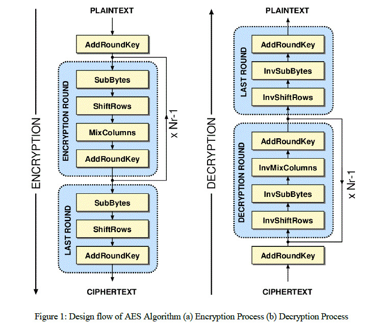 |
| Again the tenth round Inverse Mix columns stage is not included. The Overall flow of the encryption and ecryption algorithm of the AES algorithm is show in Figure1. |
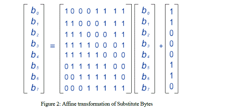
| Substitute Bytes: Is a non linear byte substitution, using a substation table (S-box) each byte from the input state is replaced by another byte. The substitution is invertible and is constructed by the composition of two transformations as described below [2] [8]. The substitute bytes operation is as shown in Figure 3. |
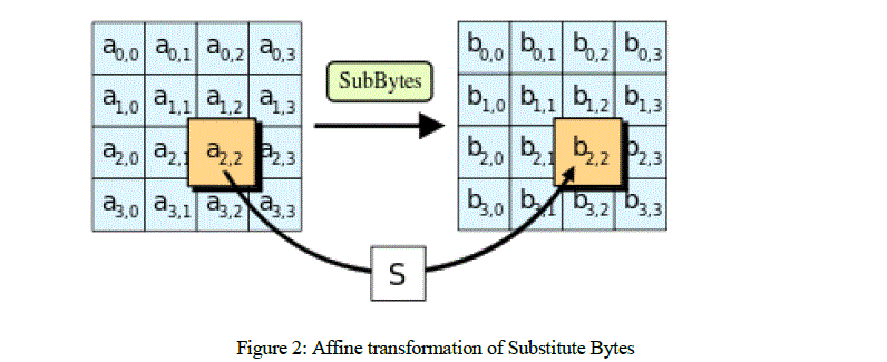 |
| 1. The state bytes are constructed by multiplicative inverse in the finite field GF (28) that is used in the AES. This field is derived using the following irreducible polynomial of degree 8: |
| m(x) = x8+x4+x3+x+1. (1) |
| 2. Affine transformation is applied on the result of above statement. The fixed matrix and the fixed vector over GF (2) in the affine transformation are shown in the Figure 2. |
 |
| Inverse Substitute Bytes: Is the reverse operation of the Substitute Bytes transformation, in which the inverse Sbox is applied to each byte of the State. This is obtained by applying the inverse of the affine transformation followed by taking the multiplicative inverse in GF (28). |
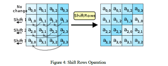
| Shift rows: In the Shift Rows transformation, the first row of the state array remains unchanged. The bytes in the second, third and forth rows are cyclically shifted by one, two and three bytes to the left, respectively as shown in Figure 4. Inverse Shift rows: Is the inverse of the shift rows, the first row of the state array remains unchanged. The bytes in the second, third and forth rows are cyclically shifted by one, two and three bytes to the right, respectively. |
 |
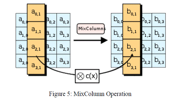
| Mix columns:In the Mix Columns transformation ,every column of the state array is considered as polynomial over GF (28). After multiplying modulo x4+1 with a fixed polynomial a(x) [2], the operation of MixColumn is as shown in Figure 5. |
| a(x)=03*x3+01*x2+ 01*x + 02 (2) |
| The result is the corresponding column of the output state is as shown in Figure 5. As it can be noticed this operation requires multiplication by „twoâÃâ¬ÃŸ and „threeâÃâ¬ÃŸ that is relatively simple shift operation in hardware. |
 |
| Inverse Mix columns: In the Inverse Mix Columns transformation, every column of the state array is considered a polynomial over GF (28). After multiplying modulo x4+1 with a fixed polynomial b(x), |
| b(x)=0B*x3 + 0D*x2 + 09*x + 0E (3) |
| The result is the corresponding column of the output state. As it not so straightforward hardware implementation as Mix column, so if we compare both, InvMixCol requires more logic resources for implementation. |
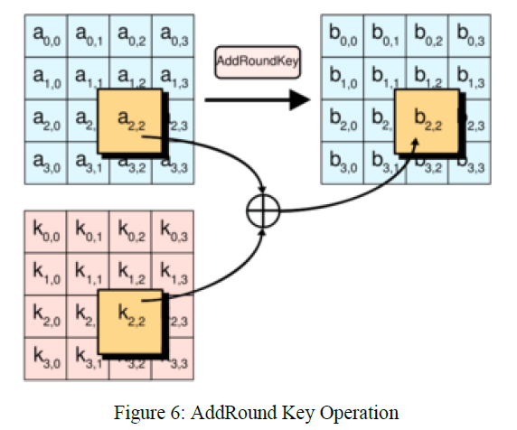
| Add Round Key: The Add Round Key operation is as shown in Figure 6, which is a simple XOR operation between the State and the Round Key. The Round Key is derived from the Cipher key by means of key schedule process. The State and Round Key are of the same size and to obtain the next State an XOR operation is done per element: |
| b (i, j) = a (i, j) ⊕ k (i, j) (4) |
| Where a is the current State, b the next State and k the round key. |
 |
| There are three steps, in each Key schedule round [6]. Keyrotate: The function Keyrotate takes a four-byte word and rotates one byte to the left. Keysubytes: The Keysubytes operation takes four-byte input word by substituting each byte in the input to another byte according to the S-Box. KeyRcon: The first byte of a word is XORed with the round constant. Each value of the Rcon table is a member of the Rinjdael finite field. Add round key is same for the both encryption and decryption. |
IMPLEMENTATION |
| A. AES Encryption : |
| To implement the AES algorithm using VHDL coding in the Xilinx 12.4 [3], we proceed with the encryption and decryption with 128 bits. The AES Encryption block is as shown in Figure 7, the encryption parameters are the input plaintext, the key of size key size and the output cipher text. First, we have to map the 16 byte input plaintext in the correct order to the 4*4 byte state, calculate the number of rounds based on the key Size and expand the key using our key schedule. At round one plaintext and key is XORed, the remaining nine rounds which has to apply all four operations: Substitute Bytes, Shift rows, Mix columns, Add round key. |
| The tenth round Mix columns stage is not included and round key was generated during each iteration [7]. Here simple XOR of each byte of the key with the respective byte of the state is done to get cipher text of the Encryption algorithm. |
| B. AES Decryption: |
| For AES Decryption, the same encryption process occurs simply in reverse order. The decryption block is as shown in Figure 8, the encryption parameters are the input cipher text, the key and the output plaintext should be same as encryption input. In decryption the key schedule remains the same; the only operations we need to implement are the Inverse subBytes, shiftRows and mixColumns, while addRoundKey stays the same. |
| EDK IMPLEMENTATION OF AES ALGORITHM: |
| In this chapter we had already seen the implementation of AES algorithm using SOFTWARE and HARDWARE individually. In those implementations some disadvantages are there. Disadvantages of software implementation overcome by hardware implementation and disadvantages of hardware implementation can be overcome by using EDK implementation. In EDK implementation we use both software and hardware combinely. |
| Embedded design in an FPGA: |
| For this design process we can use MICROBLAZE which is a softcore processor and we use SPARTAN 3E starter kit as FPGA kit for the synthesis purpose. |
| The Embedded Development Kit (EDK): |
| The Embedded Development Kit (EDK) is a suite of tools and IP that you can use to design a complete embedded processor system for implementation in a Xilinx FPGA device. |
| Xilinx Platform Studio (XPS): |
| Xilinx Platform Studio (XPS) is the development environment used for designing the hardware portion of your embedded processor system. You can run XPS in batch mode or using the GUI, XPS is now integrated with PlanAhead tools, making development easier. |
| Software Development Kit (SDK): |
| The Software Development Kit (SDK) is an integrated development environment, complementary to XPS, that is used for C/C++ embedded software application creation and verification. SDK is built on the Eclipse open-source framework and might appear familiar to you or members of your design team. For more information about the Eclipse development environment Typically, the ISE Design Tools development software is used to add an Embedded Processor source, which is then created in XPS using the Base System Builder. |
| Selecting a Board Type: |
| The BSB requires the selection of an available development board, or a custom board. Supported development boards can be selected in Project Navigator, or if starting in XPS, in the BSB introduction screens. |
| XPS Tools: |
| XPS includes the underlying tools you need to develop the hardware components of an embedded processor system |
| Platgen: |
| XPS includes the Hardware Platform Generation tool, Platgen, which generates HDL and lower level netlists for the embedded processor system. When you implement the FPGA design in the PlanAhead™ design tool, Platgen automatically runs if necessary. |
| Converting the Hardware Platform to a Bitstream: |
| For a design to work in an FPGA, it needs to be converted to a bitstream. This conversion is the following three-step process: |
| 1. XPS generates a netlist that is representative of your embedded hardware platform. |
| 2. The design is implemented (mapped into FPGA logic) in the PlanAhea tool. |
| 3. The implemented design is converted to the bitstream that can then be downloaded to the FPGA. |
| Configuring the FPGA: Download the bitstream |
| – Input file → download.bit |
| – This downloads the download.bit file onto the target board using the Xilinx |
| iMPACT tool in batch mode |
| – XPS uses the etc/download.cmd file for downloading the bitstream |
| • The download.cmd file contains information such as the type of cable is used and the position of the FPGA in a JTAG chain. |
RESULTS |
| Encryption Process (128 bit) : |
| Plain Text: 3658001543081a4f0a0c42130b3a0c00. |
| Key: 000102030405060708090a0b0c0d0e0f. |
| Cipher Text: 61d03aeddde79bdbda779bcaf0abfffe. |
| Decryption Process (128 bit) : |
| Cipher Text: 61d03aeddde79bdbda779bcaf0abfffe. |
| Key: 13111d7fe3944a17f307a78b4d2b30c5. |
| Plain Text: 3658001543081a4f0a0c42130b3a0c00. |
CONCLUSION |
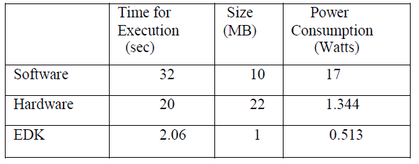
| We studied about Micro Blaze and evaluated it using small programs. We implemented AES algorithm in all three modules, which are software platform ,hardware platform and mixing of software and hardware platforms i.e using microblaze processor. Implementing AES algorithm using EDK(embedded development kit) is the better solution than the Hardware implementation and Software implementation. The execution speed is more, Power consumption is less and size required for implementation on FPGA is less when compared to Hardware implementation. |
| COMPARISION: |
 |
| FUTURE SCOPE: |
| In this project we had done the implementation of AES Algorithm.We can extend this implementation to image encryption and decryption using AES algorithm. |
References |
|