In this paper the design of feedthrough logic with improved power-delay product is presented. Feedthrough logic (FTL) is a logic design technique of the dynamic logic family. This technique solves the problems of Domino logic such charge sharing and use of inverter at the output of every stage while cascading. The proposed circuit reduces the power dissipation of the existing high speed feedthrough circuit by 30.5% for the chain of 5 inverters. The circuit is simulated in Cadence tools using 180 nm technology library.
Keywords |
| Feedthrough logic, high performance logic design. |
INTRODUCTION |
| Low power and high speed are the two most important constraints in designing VLSI circuits. High speed can be
obtained using dynamic circuits. Domino logic is the most popular dynamic logic circuit but it suffers from the
problems of charge sharing and it needs inverter at output of every stage while cascading [1,2,3]. To overcome these
problems Feedthrough logic was proposed [5], which was further improved for power in [6] but at the cost of delay.
Then ahigh speed feedthrough logic was proposed in [7] using dual supply. In this circuit delay was reduced highly but
its power dissipation was high. In this paper the circuit of high speed feedthrough logic is modified to reduce power
and attain a better power delay product. The next section describes the conventional and the high speed feedthrough
logic. The modified circuit is then introduced and at last the performance analysis and comparison between these has
been carried out. |
CONVENTIONAL FTL |
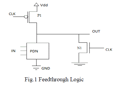
| Conventional FTL is shown in fig.1. FTL was proposed to improve the performance of domino logic. There were
some limitations in domino logic which were removed in FTL. This technique belongs to dynamic logic family.
Circuits designed with this technique consists of a pull down network (PDN), a PMOS load transistor P1 and a reset
transistor N1. Inputs are applied to the PDN block. Clock signal is connected to the gate inputs of load transistor and
reset transistor. The circuit works in two phases, reset phase and evaluation phase. In reset phase clock is high so load
transistor P1 is OFF and reset transistor N1 is ON and the output is reset to low logic level. In evaluation phase clock is
low so the load transistor P1 is ON and reset transistor N1 is OFF and the output either charges to logic high or remains
at logic low according to the inputs applied to the PDN block. |
 |
| Speed of FTL is higher than domino logic because the output logic level is evaluated before all the inputs are valid.
During cascading in domino logic a static inverter is used at the output of every stage but in conventional FTL the
output is discharged to zero level during reset phase so inverter is not required during cascading. The analysis of chain
of 10 inverters using this technique in [6] shows that during reset phase the output of each stage is at zero level and
during evaluation phase the output of each stage first goes to threshold voltage (Vth) of the transistor to which the input
from previous stage is connected and then from Vth to high level or low level according to input. As transition in this is
from Vth to high level or low level so its speed is greater. Power dissipation increases in FTL because minimum low
voltage at output is not 0V. Also noise margin is reduced in FTL as compared to domino logic [6, 7]. |
HIGH SPEED FTL |
| To further improve performance of FTL a modified FTL structure high speed (HS)-FTL was proposed in [7]. In high
speed FTL circuit the source of reset transistor Mr is connected to Vdd/2 instead of ground as shown in fig. 2. In this
circuit when clock is high Mp1 and Mp2 transistors are off and Mr transistor is on so output is charged to Vdd/2 and
when clock is low Mp1 and Mp2 are on and output is either charged to high or discharged to low according to the input
IN. In evaluation phase transition at output takes place from Vdd/2 and not zero so delay of this circuit is less. |
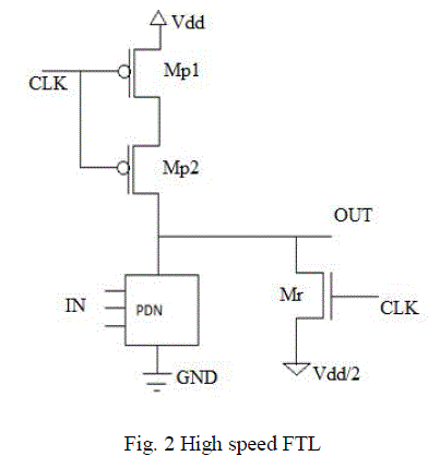 |
| The major drawback of this circuit is that during cascading when the clock signal is at high level then the output of
each stage becomes Vdd/2 which makes the transistors of next stage partially ON and there is loss of power [6, 7]. A
solution to this problem is proposed in the next section. |
PROPOSED FTL |
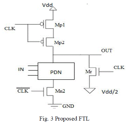
| In the above high speed FTL circuit the delay is improved highly but its power dissipation is increased. During
cascading when clock is high output of every stage is Vdd/2 which causes the transistors of next stage partially ON.
This increases the power dissipation in the circuit. To overcome this problem a transistor Mn2 is inserted whose gate is
connected to clock’ as shown in fig.3. When clock is high Mp2 is OFF and output is charged to Vdd/2 , when clock is
low Mp2 is ON along with Mp1 and Mp2 and output is either charged to high or discharged to low according to IN.
During cascading the transistors which get input from previous stage becomes partially ON because output of every
stage is at Vdd/2, so this transistor Mn2 prevents the flow of current during this time and saves the power. |
 |
PERFORMANCE ANALYSIS |
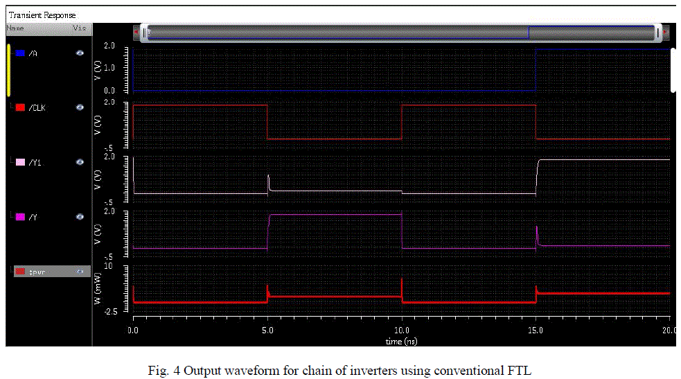
| The performance of proposed FTL circuit is verified against the existing high speed FTL [7] by designing a chain of 5
inverters. The analysis has been done using cadence design environment in 0.18μm technology library. Simulation is
done using spectre simulator. The circuit was analysed using clock frequency of 100 Mhz. Fig. 4 shows the output
waveform for the chain of inverter inverters using conventional FTL. |
 |
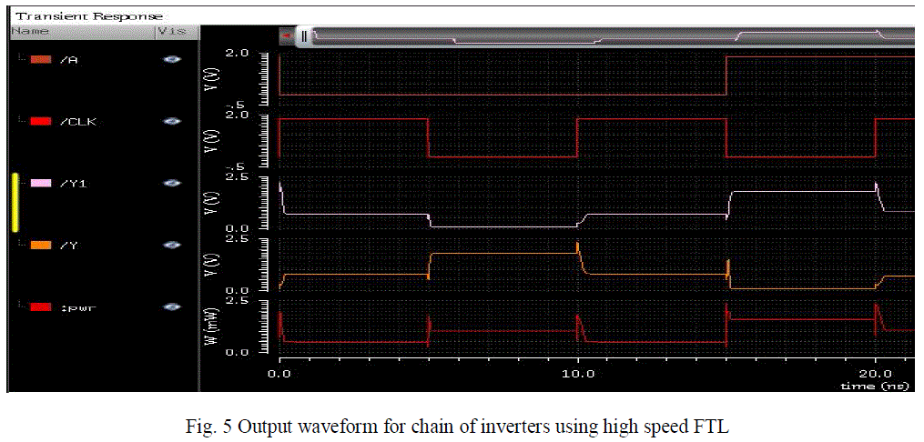
| Fig. 5 shows the output waveforms for the chain of inverters using high speed FTL. |
 |
| Fig. 6 shows the output waveform for the series of inverters using proposed FTL. From this waveform it can be seen
that the power is reduced to a greater extent. |
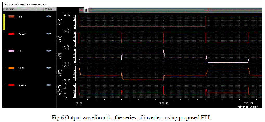 |
| In Fig. 4, 5 and 6 A is the input to the first inverter of chain of 5 inverters and Y is the output of last inverter and Y1 is
the output of second last inverter. Here pwr shows the power waveform of the respective circuit. Time scale is in
nanoseconds. |
| Table 1 shows the power dissipation, propagation delay and power delay product of the proposed FTL structure and
existing FTL and high speed FTL. |
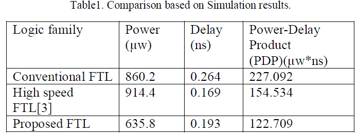 |
| From the above table we can see that high speed FTL has very less delay than conventional FTL but its power
consumption is high. Its power delay product is better than conventional FTL. Proposed FTL reduces the power
dissipation of high speed FTL by 30.5% but delay is increased slightly, so overall power-delay product is improved.
Power-delay product of the FTL structure proposed here is better than both conventional FTL and high speed FTL. |
CONCLUSION |
| From simulation results for chain of 5 inverters we can see that the proposed structure dissipate30.5% less power than
the existing high speed FTL structure. Some delay is increased due to insertion of transistor but overall power-delay
product is better than existing high speed FTL. FTL in [4] has more power dissipation so modified FTL was proposed
in [5] which reduces power dissipation but delay is high, then in [6] a high speed FTL was proposed which has very
less delay but high power dissipation, the proposed FTL structure presented in this paper reduces the power dissipation
highly and delay is slightly increased thus improving the power-delay product. |
References |
- S. M. Kang, Y. Leblebici, 'CMOS Digital Integrated Circuits: Analysis & Design', TATA McGraw- Hill Publication, 3e, 2003.
- J.M. Rabaey, A. Chandrakasan, B. Nikolic, 'Digital Integrated Circuits: A Design perspective', 2e Prentice-Hall, Upper saddle River, NJ, 2002.
- Neil H.E. Weste, David Harris and Ayan Banerjee, "CMOS VLSI Design, A circuits and systemperspective", 3rd Edition, Pearson Education, 2005.
- Kaushik Roy, Sharat C. Prasad , "Low-Power CMOS VLSI Circuit Design", John Wiley & Sons, 2009.
- V. Navarro-Botello, J. A. Montiel-Nelson, and S. Nooshabadi, âÃâ¬ÃÅAnalysis of high performance fast feedthrough logic families in CMOS,âÃâ¬Ã IEEE Trans. Cir. & syst. II, vol. 54, no. 6, pp. 489-493,Jun. 2007.
- SauvagyaRanjanSahoo, Kamala KantaMahapatra," Performance Analysis of Modified Feedthrough Logic for Low Power and High Speed", IEEE-International Conference On Advances In Engineering, Science And Management (ICAESM -2012) March 30, 31, 2012.
- SauvagyaRanjanSahoo , Kamala KantaMahapatra," An Improved Feedthrough Logic for Low Power Circuit Design", 1st IntâÃâ¬Ãâ¢l Conf. on Recent Advances in Information Technology | RAIT-2012 |.
|