International Journal of Advanced Research in Electrical, Electronics and Instrumentation Engineering
ISSN ONLINE(2278-8875) PRINT (2320-3765)
ISSN ONLINE(2278-8875) PRINT (2320-3765)
N.Indhumathi1 and Dr.S.Nirmala2
|
| Related article at Pubmed, Scholar Google |
Visit for more related articles at International Journal of Advanced Research in Electrical, Electronics and Instrumentation Engineering
Data driven clock gating is a popular technique used in many synchronous circuits for reducing dynamic power dissipation. Power optimization plays the important role in the recent years. Clock gating is a popular technique used in many synchronous circuits for reducing dynamic power dissipation.Gating manually inserted into the register transfer level (RTL) design. when a logic unit is clock, its underlying sequential elements receive the clock signal regardless of whether or not they will toggle in the next cycle. In this flip-flops are grouped so that they share a common clock enabling signal to reduce the hardware overhead. It is observed that the commonly used synthesis based gating still leaves a large amount of redundant clock pulses. In these d-flip flops are used to grouping for reducing the power. Here the Xilinx software tool will be used for implementing this proposal system.
Keywords |
| Clock gating, clock networks, dynamic power Reduction |
INTRODUCTION |
| One of the major dynamic power consumers in computing and consumer electronics products is the system’s clock signal, where it takes 30%–70% of the total dynamic power consumption [1]. There are many techniques used to reduce the dynamic power are developed, in which clock gating is predominant. Ordinarily, when a logic unit is clocked, it is based on the sequential elements receiving the clock signal, sequentially they will toggle in the next cycle whether it is required or not. With clock gating, the clock signals are ANDed with explicitly predefined enabling signals. Clock gating is employed at all levels: system architecture, block design, logic design, and gates [2], [3]. Several methods to take advantage of this technique are described in [4]–[6], with all of them depending on various heuristics in an attempt to increase clock gating opportunities. With the rapid increase in design complexity, computer aided design tools supporting system-level hardware description have become commonly used. Although substantially increasing design productivity, such tools require the employment of a long chain of automatic synthesis algorithms, from register transfer level (RTL) down to gate level and net list. Unfortunately, such automation leads to a large number of unnecessary clock toggling, thus increasing the number of wasted clock pulses at flip-flops (FFs). |
| In a recent paper, a model for data-driven gating is developed based on the toggling activity of the constituent FFs [9]. The optimal fanout of a clock gater yielding maximal power savings is derived based on the average toggling statistics of the individual FFs, process technology, and cell library in use. In general, the state transitions of FFs in digital systems depend on the data they process. Assessing the effectiveness of data-driven clock gating requires, therefore, extensive simulations and statistical analysis of the FFs’ activity. Another grouping of FFs for clock switching power reduction, called multibit FF (MBFF). MBFF attempts to physically merge FFs into a single cell such that the inverters driving the clock pulse into its master and slave latches are shared among all FFs in a group. MBFF grouping is mainly driven by the physical position proximity of individual FFs, while grouping for data driven clock gating should combine toggling similarity with physical position considerations. While answered the question of what is the group size that maximizes power savings, this paper studies the questions of: 1) which FFs should be placed in a group to maximize the power reduction and 2) how to algorithmically derive those groups. Implementation .In the next section, we briefly overview data-driven clock gating, which motivates this paper.. Section III introduces layout considerations into FF grouping and describes a near-optimal grouping algorithm. Section IV presents the problem of optimal FF grouping and its inheren difficulty. Section V discusses the implementation of a practical design flow. Section VI presents experimental results obtained for digital signal processor (DSP) and 3-D graphic designs. Final conclusions are presented in Section VII. |
DATA-DRIVEN CLOCK GATING |
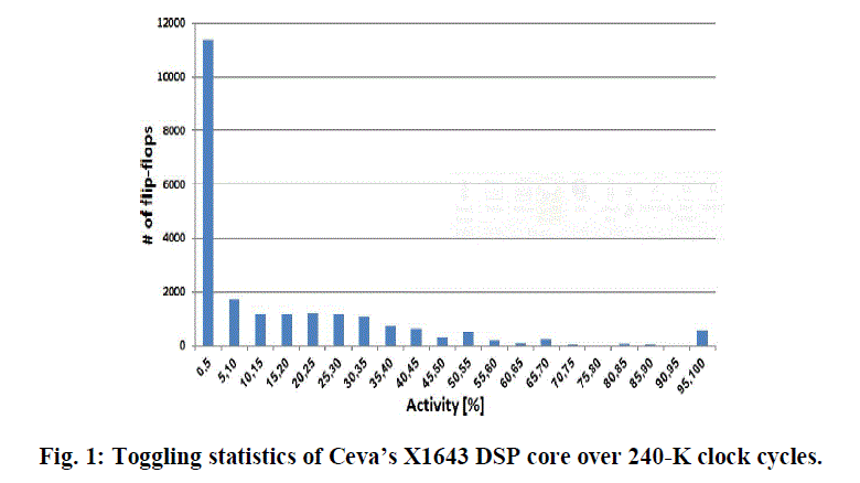
| Clock enabling signals are very well understood at the system level and thus can effectively be defined and capture the periods where functional blocks and modules do not need to be clocked. Those are later being automatically synthesized into clock enabling signals at the gate level. In many cases, clock enabling signals are manually added for every FF as a part of a design methodology. Still, when modules at a high and gate level are clocked, the state transitions of their underlying FFs depend on the data being processed. It is important to note that the entire dynamic power consumed by a system stems from the periods where modules’ clock signals are enabled.. Fig. 1 shows the FFs’ toggling activity in an arithmetic block comprising 22K FFs, designed in 40-nm technology ,taken from Ceva’s X1643 DSP core for multimedia and wireless baseband applications The statistics is obtained from extensive simulations of typical modes of operation, consisting of 240-K clock cycles. when the FFs clock signal is enabled is only 10%, which is still responsible for the entire dynamic power consumed by that block. The clock enabling signals are obtained by RTL synthesis and manual insertions. As Fig. 1 shows, a FF toggled its state only 2.9% of the clock enabled time period, on the average, thus more than 97% of the clock pulses driving FFs are useless. |
 |
| A FF finds out that its clock can be disabled in the next cycle by XOR ing its output with the present data input that will appear at its output in the next cycle. The outputs of k XOR gates are ORed to generate a joint gating signal for k FFs, which is the n latched to avoid glitches. The combination of a latch with AND gate is commonly used by commercial tools and is called integrated clock gate (ICG). Such data driven gating is used for a digital filter in an ultralow-power design. A single ICG is amortized over k FFs. There is a clear tradeoff between the number of saved (disabled) clock. pulses and the hardware overhead. With an increase in k, the hardware overhead decreases but so does the probability of disabling, obtained by OR ing the k enable signals. Let the average toggling probability of a FF (also called activity factor) be denoted by p (0 < p < 1). The latch and gater (AND gate) overheads are amortized over k FFs. It is shown in [9] that the number k of jointly gated FFs for which the power savings are maximized is the solution of |
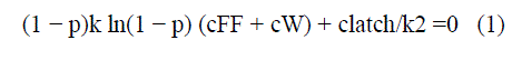 |
| where cFF is the FFs clock input capacitance, cW is the unit-size wire capacitance ,and clatch is the latch capacitance including the wire capacitance of its clk input. Such a gating scheme has considerable timing implications, which are discussed in [9]. We will return to those when discussing the implementation of data-driven gating as a part of a complete design flow. For the scheme proposed in Fig. 2 to be beneficial, the clock enabling signals of the grouped FFs should preferably be highly correlated. Data-driven clock gating is shown to achieve savings of more than 10% of the total dynamic power consumed by the clock tree It took advantage of the very low dynamic range of the data in a digital filter. The gating logic is tailored to the structure of the filter, whereas the approach discussed in this paper is more general and applies to large scale and a wide range of designs. |
 |
PHYSICAL LAYOUT CONSIDERATIONS IN FFS GROUPING |
| Finding sets of FFs that minimize the number of redundant clock pulses is not enough to maximize power savings. Grouping must account for the on-die locations of FFs and gaters, which affect the power consumption due to the capacitive loads resulting from their connections. The physical locations of FFs affect also the delay and clock skew, and it is therefore desirable for FFs driven jointly by the same clock gater, to be placed in proximity of each other. and energy consumption are calculated. |
 |
OPTIMAL FFS GROUPING FOR JOINT CLOCK GATING |
| Knowing the optimal group size k, the next step is to partition the FFs of a system into k-size sets such that the power savings will be maximized .Such tools are focusing on skew, power, and area minimization, but they are not aware of the toggling correlations of the underlying FFs, which this paper is focusing on. The optimal value of k is obtained from (1) under toggling independence assumption, but in reality the toggling may be correlated, so in practice one can expect higher saving than the theoretical lower bound obtained under independence assumption. A practical design methodology should preserve the integrity of system clock enabling signals. This means that the FFs of a k-size set must all belong to the same enabled clock (called hereafter pre-enabled). |
| A bottom-up process for a coarse, block-level gating is proposed in [5] by repeating the MCPM algorithm. We have adapted this idea to FF-level gating. Starting with n individual FFs and constructing the associated n-vertex FF pair wise activity graph, an MCPM algorithm then finds the best FFs pairing. A new n/2-vertex pair wise activity graph is then defined where its vertices correspond to the matching (n/2 edges) found in the former step. The process repeats K times until groups of size k = 2K are determined. For k = 2(K = 1), MCPM indeed solves the problem of minimizing the number of redundant clock pulses, but its repetitive application for k > 2 (K > 1) may not find the minimum, as otherwise this would contradict the NP-hardness. Still, the iterative MCPM algorithm is practical and has acceptable run time. |
IMPLEMENTATION AND INTEGRATION IN A DESIGN FLOW |
| In the following, we describe the implementation of data driven clock gating as a part of a standard backend design flow. It consists of the following steps. |
| 1) Estimating the FFs toggling probabilities involves running an extensive test bench representing typical operation modes of the system to determine the size k of a gated FF group by solving (1). |
| 2) Running the placement tool in hand to get preliminary preferred locations of FFs in the layout. |
| 3) Employing a FFs grouping tool to implement the model and algorithms presented in Sections III and IV, using the toggling correlation data obtained in Step 1 and FF locations’ data obtained in Step 2. The outcome of this step is ksize FF sets (with manual overrides if required), where the FFs in each set will be jointly clocked by a common gater. |
| 4) Introducing the data-driven clock gating logic into the hardware description (we use Verilog HDL). This is done automatically by a software tool, adding appropriate Verilog code to implement the logic described in Fig. 2. The FFs are connected according to the grouping obtained in Step 3. A delicate practical question is whether to introduce the gating logic into RTL or gate level description. This depends on design methodology in use and its discussion is beyond the scope of this paper. We have introduced the gating logic into the RTL description. |
| 5) Re-running the test bench of Step 1 to verify the full identity of FFs’ outputs before and after the introduction of gating logic. Although data-driven gating, by its very definition, should not change the logic of signals, and hence FFs toggling should stay identical, a robust design flow must implement this step. |
| 6) Ordinary backend flow completion. From this point, the backend design flow proceeds by applying ordinary place and route tools. This is followed by running clock tree synthesis. |
| Few timing-related comments are in order. The extra gating delay introduced by the feedback loop in Fig. 2 should not exceed the delay margins of paths from the clock input clk_g of FF1 to the data input D2 of FF2. In ordinary designs, notably in automatically synthesized blocks, most of the delay margins are large enough to absorb the introduction of the gating logic. If at a later stage timing violations due to the gating are found, one can simply drop the data-driven gating from the troublesome FFs. We found very few of those in our designs, less than 5% of the FFs. Relaxation of the clock cycle can also overcome this problem, but it must be considered in a wider context of powerdelay trade off and product specifications, which is beyond the scope of this paper. |
SIMULATION RESULTS |
| The design flow described in Section IV is experimented on a DSP core comprising 22 k FFs (Fig. 1), another large vectored DSP core comprising 100 k FFs, a 3-D graphics accelerator [9], and a network processor control block. For FF toggling probabilities from p = 0.01 to p = 0.05, the group size maximizing the net power savings is The latter is due to the very low toggling rate of that processor. As shown in the tables, the net dynamic power savings are 15% for the DSP cores and 20% for the 3-D graphics accelerator. Experiments for the network processor control block also yield nearly 20% power savings where the optimal group size is k = 8. between k = 8 and k = 4. We measured the power savings compared with the nominal designs using the Spy Glass EDA power simulator [8]. |
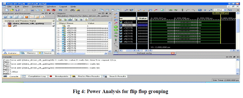
| Fig 4 shows that the output waveform for data driven clock rating with carry skip adder. Here to give a 24 bit d1 and d2 input bits and get a 24 bit s0 and s1 output bits. The output waveform s0 indicates sum of the d1 and d2 inputs then next clock pulse to obtain the same input s1. |
 |
| It is interesting to compare the relative power savings achieved by applying synthesis-based gating only or data driven gating only or both. To this end, we ran RTL power simulation of the processors in four gating modes: |
| 1) no gating; |
| 2) synthesis-based available from an EDA vendor ; |
| 3) data-driven; and |
| 4) both combined. |
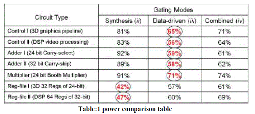
| Summarizes the total power consumption of each case and compares it with the native design without any gating [shown in (1)]. The synthesis-based gating alone 2) reduced the total power to 84%, 34%, and 59%, respectively. Applying data-driven gating on top of the synthesis-based one 4) further reduced the power to 68%, 29%, and 50%, respectively. However, for all three designs, the application of data driven gating alone yielded higher power savings than the combination of data-driven and synthesis-based, reduction the power to 65%, 27%, and 42%, respectively. This is due to the fact that data-driven gating stops any unnecessary clock pulse, and the inclusion of the synthesisbased gating only adds logic circuits that becomes redundant once the data-based gating is applied. Although synthesisbased clock gating is a well-established design methodology, the above experiments encourage its replacement by datadriven gating. To further characterize the benefits of the two gating modes, we analyzed several different circuit types, for example, control units, arithmetic units, and register files. |
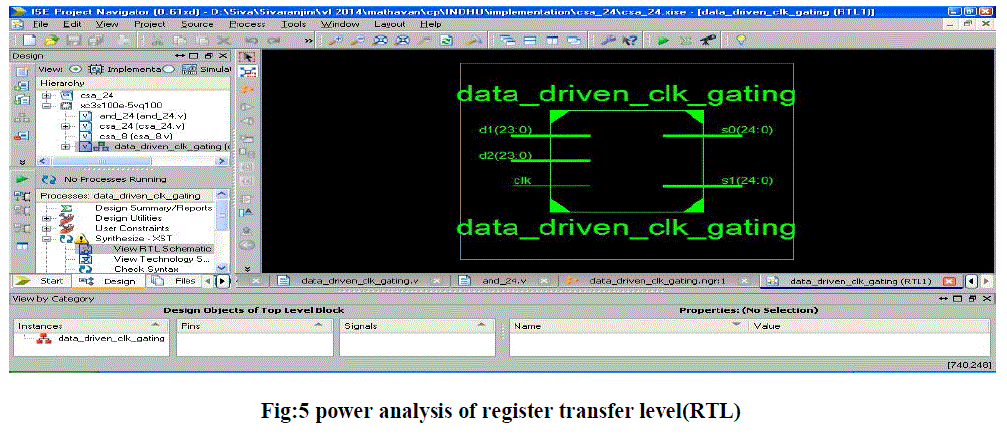
| Fig 5 shows |
 |
| To further characterize the benefits of the two gating modes, we analyzed several different circuit types, for example, control units, arithmetic units, and register files. We selected such units from the large designs that we analyzed above, where the type of the circuit is specified. The resulting power consumptions (in percentages), are relative to the no clock gating case, and the lowest power is indicated in red (circled). It can be seen that for control circuits, data-driven gating 3) is outperforming synthesis-based gating 2). This is explained by their very low toggling rate, where datadriven is most useful. Similar behavior is observed for arithmetic circuits (their IO registers are included). Expectedly, synthesis-based gating is still favored for register files. This follows since only one register is changing its data at a time, a condition that can easily be caught and defined in the RTL code. |
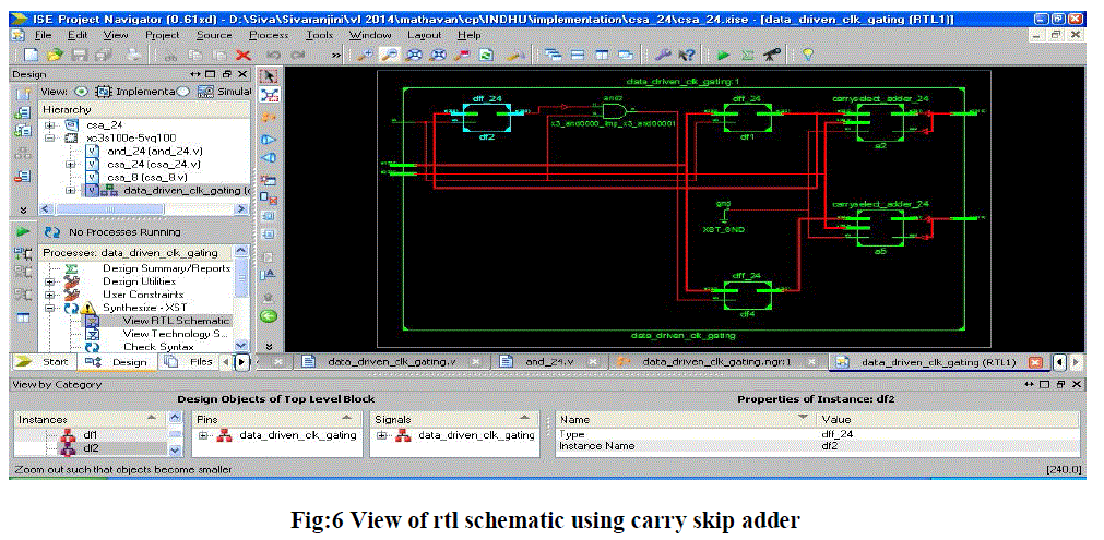 |
| Fig 6 shows that the RTL schematic diagram for data driven clock rating with carry skip adder using Xilinx tool from this we obtain the logic and gate block of the following synthesis code |
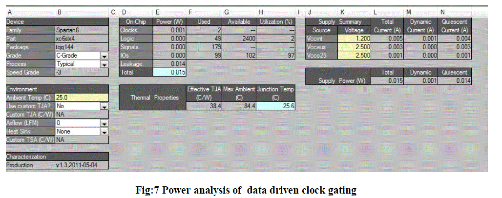 |
| Fig.7 shows the power analysis for the data driven clock rating with carry skip adder. Here mention supply power, leakage power, dynamic current and quiescent current. |
| It can be seen that for control circuits, data-driven gating 3) is outperforming synthesis-based gating 2). This is explained by their very low toggling rate, where data-driven is most useful. Synthesis -based gating is still favoured for register files. This follows since only one register is changing its data at a time, a condition that can easily be caught and defined in the RTL code. Therefore, applying data driven gating on top of synthesis-based mostly adds circuit overhead. The results of the combined synthesis-based and data-based gating scheme are worse than the data-driven only gating for all seven circuits. Thus, unless register files can undergo only synthesis-based gating and data-based gating will not be applied to them, synthesis-based gating should be completely replaced by data-based gating. |
 |
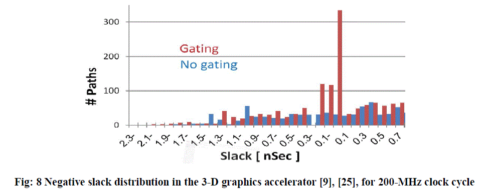
| Fig. 8 illustrates the margin (slack) distribution for 200-MHz clock cycle. It can be seen that the margin distribution has slightly worsened as more paths now have a negative slack. The violations need to be taken care of for timing closure and a variety of actions and techniques are possible, but their discussion is beyond the scope of this paper. |
 |
CONCLUSION |
| This project studied the problem of grouping FFs for joint clocking by a common gater to yield maximal dynamic power savings. Although the problem was NP-hard, several practical algorithms to solve it and found several of them to be useful in a real design automation implementation. The solution was integrated in a practical design flow. In Future going to use carry select adder instead of carry skip adder. Experimental results of DSP cores, a network processor control block, and a 3-D graphics accelerator were presented, achieving 15%–20% total power reduction. The FF grouping problem also arised in MBFF, where distinct FFs were combined in one physical cell to share their internal clock drivers. It is interesting to consider the combination of data-driven gating with MBFF in an attempt to yield further power savings. |
References |
|