International Journal of Advanced Research in Electrical, Electronics and Instrumentation Engineering
ISSN ONLINE(2278-8875) PRINT (2320-3765)
ISSN ONLINE(2278-8875) PRINT (2320-3765)
V.Prasanth1 and K.V.Rajeshkumar2
|
| Related article at Pubmed, Scholar Google |
Visit for more related articles at International Journal of Advanced Research in Electrical, Electronics and Instrumentation Engineering
RISC is a design philosophy to reduce the complexity of instruction set that in turn reduces the amount of power consumption, space, cycle time, cost and other parameters taken into account during the implementation of the design. The advent of FPGA has enabled the complex logical systems to be implemented on FPGA. The intent of this paper is to design and implement 64 bit RISC processor using FPGA Spartan 3E tool. This processor design depends upon design specification, analysis and simulation. It takes into consideration very simple instruction set. The momentous components include Control unit, ALU, shift registers and accumulator register. Power consumption reduced by designing clocking techniques.
Keywords |
| RISC, control unit, processor |
INTRODUCTION |
| Now days, Computers are mainstream in quotidian activities. RISC Processor is a CPU design strategy that uses simplified instructions for higher performance with faster execution of instruction. It also reduces the delay in execution. It uses general instructions rather than specialized instructions. They are less costly to design, test and manufacture. This has helped in implementation of RISC in technological field. Its range of application includes signal processing, convolution application, supercomputers such as K computers and wider base for smart phones. |
| In this work, a 64 bit RISC processor is presented with higher performance and efficiency being the main aim. This processor comprises of Control unit, general purpose registers, Arithmetic and logical unit, shift registers. Control unit follows instruction cycle of 3 stages fetch, decode and execute cycle. According to the instruction to the fetch stage, control unit generate signal to decode the instruction. The architecture supports 16 instructions for arithmetic, logical, shifting and rotational operations. |
| The whole paper is divided into the following sections. Section I describes the architecture of the processor. Section II explains the various modules of the processor. Result has been presented in the section III |
ARCHITECTURE |
| The architecture of 64 bit RISC processor has been shown in the figure 1. It comprises of Control unit, general purpose register, ALU, Barrel shifter, universal shift register and accumulator. The control unit consists of two registers i.e. instruction register and instruction decoder. Instruction and data are fetched sequentially in order to reduce the latency in the machine cycle. Pipeline structure has been incorporated that further utilizes three execution cycle fetch, decode and execute. This pipeline structure helps in enhancing the speed of operation. In fetch cycle, instruction and relevant data are inferred from the memory while in decode cycle, instruction and data drawn from the memory are bifurcated to activate component and data path for execution and in the execution cycle instruction is executed, data is manipulated and result is stored in the accumulator. |
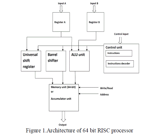 |
| The control unit accepts the opcode and generate the signal that triggers the components and data path to work accordingly and perform the desired function. The control unit has two instruction decoders. These two decoders decode the instruction bits and direct the signal to either into ALU, universal shift register or barrel shift rotator. The operands are received from register A or register B. Upon receiving the operands from registers and the decoded instruction bits arithmetic and logical unit perform arithmetic and logical functions. Universal shift register and barrel shift rotator receives the input from register A and depending upon the decoded information perform the desired operation of either shifting or rotation and the result is stored in the accumulator register. |
 |
MODULES IN THE DESIGN OF 8 BIT RISC PROCESSOR |
| Modules are the building blocks of a Processor. This segment deals with the modules of 64 bit RISC processor. Control Unit, ALU, general purpose register, universal shift register, barrel shift rotator and accumulator are main modules of the processor. |
1. Control Unit: |
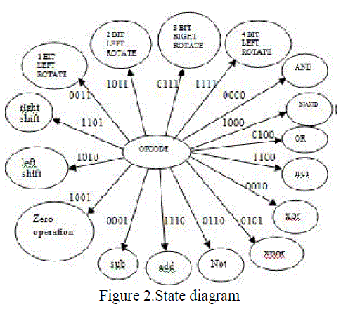
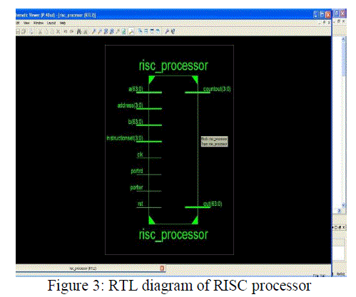
| The control unit is based on state diagram as depicted in the figure 2. The state machine performs the functions of arithmetic, logical, shifting and rotating functions. If bit instruction is 0100 then OR operation is performed as soon as next instruction is received then appropriate operation is performed. The control unit consists of two decoders. The first decoder performs arithmetic and logical function and the second decoder performs shifting and rotating operations. The top block of control unit is shown in the figure 3. |
 |
2. ALU |
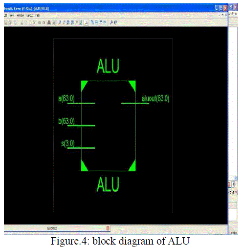
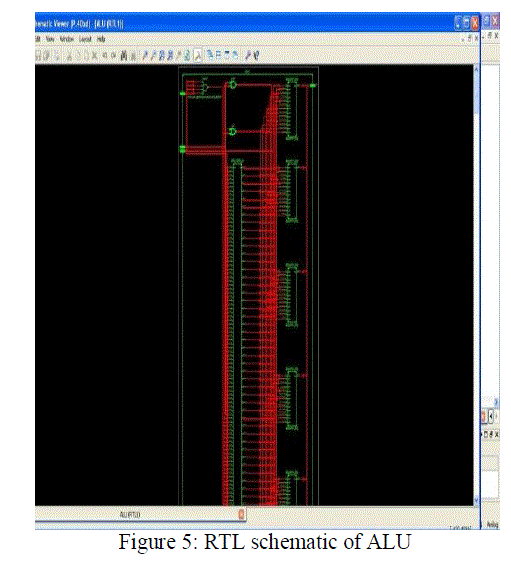
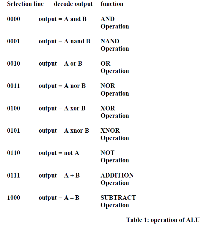
| Arithmetic and logical unit is a digital circuit that performs arithmetic and logical operations. The proposed design performs seven logical functions and two arithmetic functions. The logical operations to be executed are AND, NAND, OR, NOR, XOR, XNOR and NOT while two logical operations are performed Addition and Subtraction. ALU will receive instruction bits from control unit and will execute the desired operation. For example, if input to control unit is 0000, the decoded bits will be 64-bit data and after receiving the instruction bits from the decoder AND operation is performed by ALU according to the operands from register A and register B. The top block is shown in the figure 4. |
 |
 |
 |
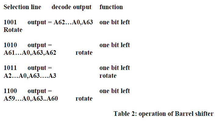
3. Barrel Shifter: |
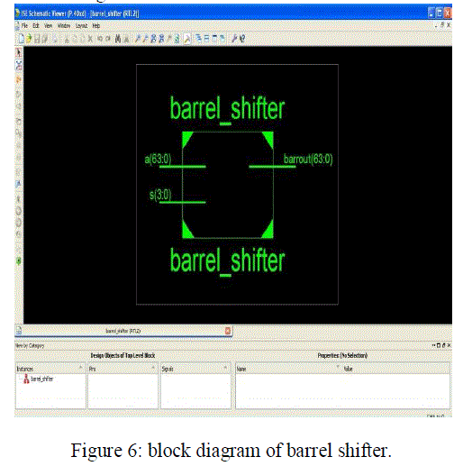
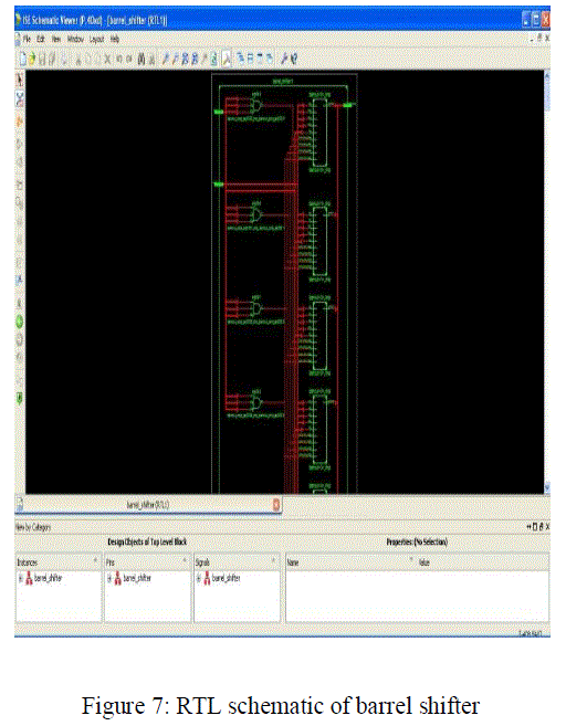
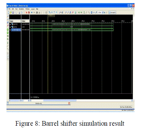
| Barrel shifter is shown in the figure 6. It is a digital circuit that shifts the number of bits by specified times. It will receive the decoded instruction bits from the second instruction decoder inside the control unit and performs the desired operation depending upon operand from register A and select lines. |
 |
 |
 |
 |
4. Universal Shift Register |
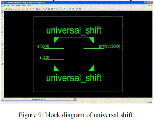
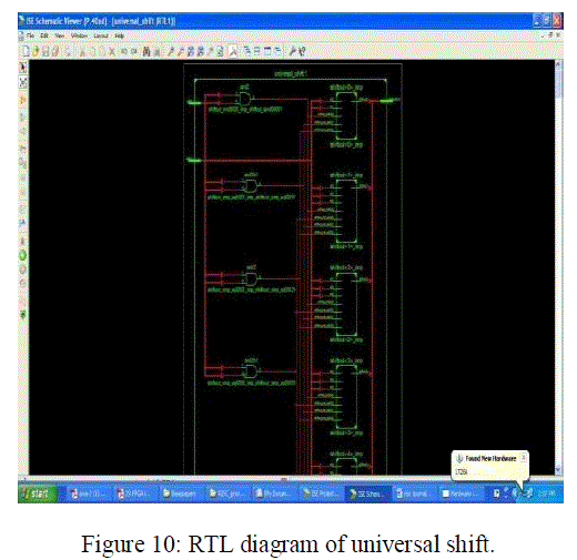
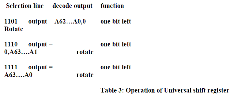
| The architecture is shown in the figure 9. This architecture performs four main functions as follows loading the value, left shift and right shift and no change. If s4 and s5 both are low while z is equal to 01000000 the value is loaded. If s4 is low and s5 is high with decoded output z as z63….z0 left shift operation is performed. |
 |
 |
 |
5. General Purpose Register |
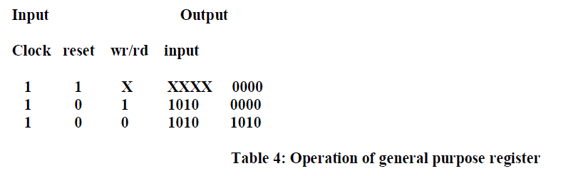
| General purpose register stores the 8 bit data. There are total 8 D flip flops. Two general purpose registers are A and B. If reset is high then register is clear, on the other hand if reset is low, rd is taken to be high and clock is high data is stored in the register. It is shown in the figure 11. |
 |
6. Accumulator Register: |
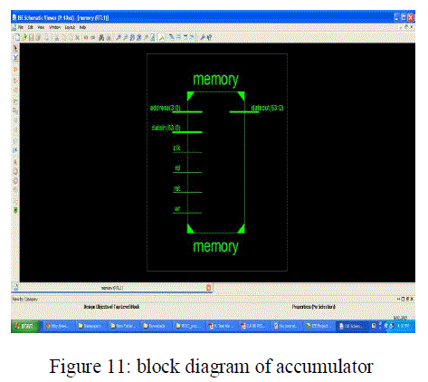
| Accumulator register top block is shown in the figure 11.The result from ALU or universal shift register or barrel rotator is stored in the accumulator register. If reset is set to high then accumulator register is cleared otherwise 64 bit result is stored in the accumulator register. |
 |
RESULT |
 |
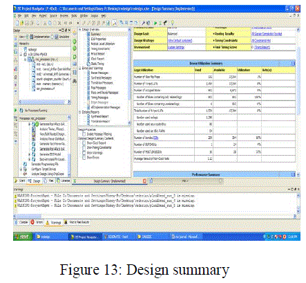 |
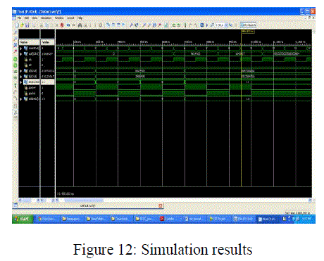
| The performance of 64 bit RISC processor has been scrutinized using Xilinx Spartan 3E technology. The design meets the requirement of high speed, extremely low cost and consumer oriented design. The overall design has been shown in the figure. The data is received from two 8 bit registers A and B. Signal READ (rd) is a memory interface signal. This signal adumbrates the memory location to be read and data to be put into the data bus. The synchronization is done utilizing clk signal. Design of processor has been accomplished using two control signals namely rd and reset. If reset is high, processor will not perform any operation and continue to remain in idle state. If reset is low and rd is high data is loaded into register. Depending upon the opcode from control unit the processor performs the operation. This 64 bit RISC processor works on one clock cycle. clk is the external clock signal and triggers the input and result in the output. rd triggers the state of registers A and B. s0 to s3 specifies the opcode to enable the operation. If opcode is 0100 then OR operation is performed. |
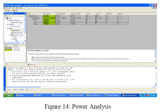
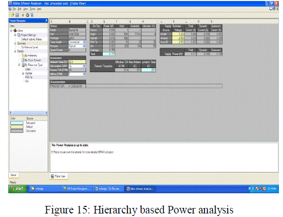
POWER ANALYSIS |
| Whereas power consumption point of view this RISC processor consumes 0.177mW within the frequency range of 1000 MHz. |
 |
 |
CONCLUSION |
| A 64 bit RISC processor with 16 instruction set has been designed. Every instruction has been executed in one clock cycle with 3 stage pipelining. Verification has been endeavored by exhaustive simulation. Power consumption also reduced by using clocking techniques, the processor can be used for mathematical computation in portable calculators as well as in gaming tool kit, signal processors, vending machines, etc. |
References |
|