International Journal of Advanced Research in Electrical, Electronics and Instrumentation Engineering
ISSN ONLINE(2278-8875) PRINT (2320-3765)
ISSN ONLINE(2278-8875) PRINT (2320-3765)
V. V. Patil1, P.A. Uchagaonkar1, Dr. S. A. Shinde2 and Dr. R. K. Kamat3
|
| Related article at Pubmed, Scholar Google |
Visit for more related articles at International Journal of Advanced Research in Electrical, Electronics and Instrumentation Engineering
DAC (Digital to Analog Converter) is the enabling inverse technology of ADC that generates analog output proportionate to given digital input. In most of the control and digital processing system requires the DAC for meddlesome with real world. But most of the digital controlling microprocessor and microcontroller don’t have an on chip DAC integrated peripheral architecture. For such implementing system, an external DAC chip is normally used but it decreases the efficiency of system such as power, cost, area. This paper reports on FPGA based Soft IP design for reconfigurable High Resolution DAC using PWM technique. FPGA (Field Programmable Gate Array) have advantage over to the traditional technology of reconfigurability, shorter time to market and non recurring cost and system on chip ability which reduces the board size with increasing efficiency. This designed soft IP core which can be used in parallel with another included FPGA based architectures.
Keywords |
| Digital-Analog Conversion, Field Programmable Gate Array, Reconfigurable Architectures, Pulse width modulation converters, Mixed Signal Analog Integrator Circuits |
INTRODUCTION |
| Since the real world signals are in analog format, there is necessity in most of the electronic system to converting in analog to digital for digital processing and again back it into digital to analog for connecting with real world. The DAC is the Digital to Analog Converter which is one of the kernel functionality in electronics system. Formerly this ADC and DAC have the special function IC interfacing with microcontroller and microprocessor for digitizing real world analog data. But the recent trend has been change to system on chip in which all components like digital, analog, mixed signal integrates into a signal chip. Taking advantage of increasing the efficiency of power, area and cost, it is very suitable for embedded application development. But in most of the microcontroller and microprocessor systems don’t have an on chip DAC module. In that case the external DAC module interfaced with implemented system which increases the cost of the system, size of the device and reduces the power efficiency also. [1,2] |
| The FPGA is the Field Programmable Gate Array are advantage over the technology of reconfigurability, shorter time to market capability and system on chip ability which reduces the cost, board size with increasing efficiency. The FPGAs are widely used in digital signal processing area and for that it often needs the data converters for meddlesome with real world. Looking to the immense importance of it, the high resolution digital to analogue converter (DAC) has implemented on the FPGA paradigm. The PWM technique is one of the famous techniques for implementing the DAC functionality in digital area. This paper focus and reports on FPGA based reconfigurable high resolution DAC design using PWM technique. This designed soft IP can be used as in FPGA based design architectures. It provides high degree of flexibility and reduces cost of system avoiding external circuitry and time to market.[4] At the beginning of the paper recent advances and pertaining prior research work is interpreted in section II. |
| The rest of the paper illustrates implementation of DAC Soft IP, Section III describes the concept of presented PWM based DAC architecture. Section IV and V focuses on research problem with implementation details related with design. And section VI reveals the results and conclusion of the system. |
RELATED WORK |
| The research work is regarding the rec-configurable audio sigma-delta DAC on the FPGA paradigm for the embedded applications design reported by Ray C. C. Cheung et. al [10]. In this paper, he has explained and designed the 3rd or 5th order sigma delta modulator by allowing varying sampling rate with the programmable interpolator. While this DAC accepts above 16 bit to 24 bit PCM data sample rate at the specific KHz range frequencies which is suitable with in applications of CD, SACD, and DVD audio. [9] Notably design issues are explored by Hugo Cheung et. al[10] is that, at the time of opted the DAC for an different application; the designer have to consider the performance characteristics of the DAC such as its resolution, full scale voltage, output bitstream and average of analog output voltage. Another researcher Puidokas et. al.[12] also report on the structure of 1-bit DAC implementation on FPGA by realizing interpolator and modulator. It improved the dynamic range of noise shaping loop and diminish the need of external analogue filter. Pertaining for this the hardware-software co-design simulation was performed using integrated Matlab simulink package of Xilinx system generator, Xilinx ISE and modelsim. The design of Digital sigma delta modulator is the crucial part of this type of DAC accordingly classified as per the order, configuration of noise shaping and the type of feedback signal. Alternative solution is explained and reported by Patel et. al. [11], on the FPGA based PID controller for dynamic system. To control this system the digital output converted in the real world analog format by driving the DAC with the pulse width modulation technique on FPGA paradigm. Based on this concept we are designed generalised soft IP core of reconfiguration DAC which detail described in the further section. |
PROPOSED METHODOLOGY AND DISCUSSION |
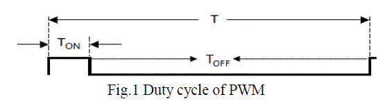
| Pulse Width Modulation is the form of digital signal modulation technique with fixed frequency but varying duty cycle. If the duty cycle of the PWM signal is varying with time and the output of signal filter with simply using RC low pass filtering, it generates the analog signal.[1]So using this technique it is possible to design on chip a high resolution reconfigurable DAC which can fills the role. The resolution of the DAC is equivalent to the resolution of the PWM signal. The DAC sample rate is same as duty cycle of PWM. The duty cycle of PWM is shown in fig 1 as, |
 |
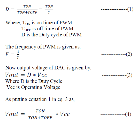 |
| So as per eq. (4) shows that output voltage directly proportional to the ON time. This PWM can be implemented as on incrementing timer and other compare registers which changes output on external hardware pin when compare match as shown in fig. 2. |
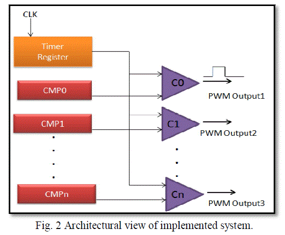 |
| DAC Resolution is equal to the Timer resolution and is equivalent to the timer width. The digital value which is to be converted into analog value is stored in compare register (CMP Register) which continuously compared with Timer value by respected Comparator. The corresponding pin state is changed by comparator with respect to comparator output. Getting output voltage is filtered with external filtering circuitry which generates analog value to corresponding digital value. For example, for 16 bit DAC implementation, Timer and Compare Register should be 16 bit. Consider here data value which is converted in analog format is 0x4A3D then Compare Register is filled up with 0x4A3D and timer start incrementing from 0x0000. The output pin becomes high when just timer start and still remains high upto timer matches with compare register data value which is 0x4A3D. At this matching point output state is change to zero. This operation repeats for each cycle. This produces PWM with desired Duty Cycle. For one sample to convert from digital to analog takes 1 timer overflows or 1 PWM operating cycle. For 16 bit timer it has count up to 65536 times or 8 bit it has 256 counts. |
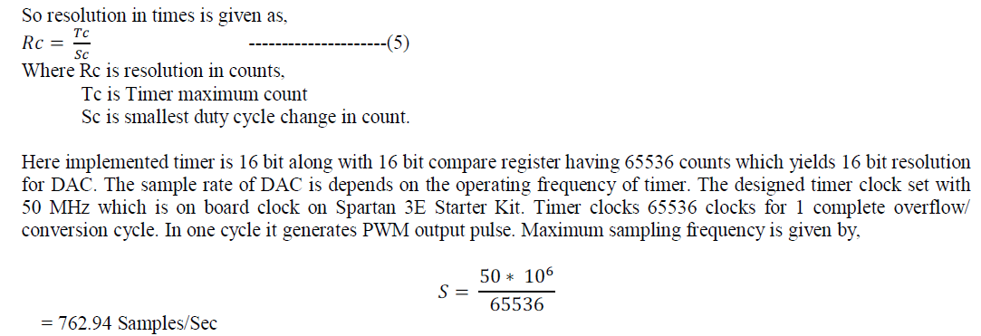 |
| For 16 bit Resolution we get 762 samples per second. As resolution increases sampling rate decreases. For 8 bit resolution the maximum sample rate can be 195k/sec. The relation between sampling rate and resolution is inversely proportional. As resolution increases the sampling rate decreases. And as sampling rate increases the resolution decreases. |
SCOPE OF RESEARCH |
| This mixed signal system requires real world analog signal should be converted to digital domain , which normally done ADC and after digital signal processing and decision making the same digital data is converted back to analog domain using DAC, for driving actuators. Use of such external data converters are increases cost power consumption, board size and design complexity. FPGA works with only digital data with reconfigurable blocks requiring external DAC to generate analog signal. Pulse width modulation is one of the techniques which used to generate analog data removing need of DAC in digital domain. PWM techniques can be implemented on traditional hard cored microcontrollers using on chip fabricated peripherals like timers and counters. This implementation on microcontroller have disadvantages like; they should program and realized in software with increasing code size, system complexity with increasing numbers on interrupts and increasing power consumption due to increased wake ups from low power mode. Some time desired resolution and accuracy cannot be obtained due to interrupt latencies and system context switching. As these hard wired devices have fixed size timer width from it generated fixed resolution PWM without providing flexibility to programmer for changing it as per need. Peripheral Timers also limited in numbers with fixed number of channels with limited compare registers for providing output PWM due to fixed resources. These limitations put constraint on maximum implementations of parallel operating DACs. These microcontrollers have hard wired output pins IOs for PWM generation which cannot be changed by programmer, making PCB designing very difficult with increasing complexity. Software implemented DACs has very low sampling rate because of microcontrollers low operating frequency. |
| On other hand new approaches like FPGA have many advantages over traditional one like reconfigurability, high flexibility, sea of gates along with high operating frequency, with increased computing power. In FPGA implementations, DAC can be designed with reconfigurability functionality having facility to change resolution, sampling rate and numbers of DACs. As everything in FPGA is hardwired and do not have software operating parts, FPGA implementation do not have problems of interrupt latencies, context switching. Due to this benefit Implemented DAC has accurate and precise output PWM. These implemented DACs are IPs working and implemented in hardware with operating in parallel with another applications which reduces system complexity, which rises due to sequential and interdependent programming in traditional software methods. It is very easy to handle and configure these DACs due to just simple parallel interface DATA bus, giving very simple communication way and high simplicity. This is not in case with external DAC chips which have many signals and different communication interfaces like I2C, SPI. FPGA is Sea of gates with reconfiguration capacity, we can implement numbers of parallel operating DACs as per need and requirement, efficiently utilizing on chip resources. FPGA has high flexibility with working with IO pins. IO pins are fully programmable providing programmer flexibility to connect any signal to any desired external IO Pin, reducing PCB design complexity. |
IMPLEMENTATION AND EXPERIMENTAL RESULTS |
| The soft IP is designed with keeping aim in mind that it should be easily interfaced with other applications and IPs running on FPGA concurrently. This DAC soft IP is implemented using high level hardware descriptor language Handel C. Handel C is HDL with traditional C syntax with some changes. It has simplicity and benefits of C language, while producing optimized and efficient hardware like traditional HDLs VHDL and Verilog. Handel C provides great simplicity and reliability in describing hardware than other HDLs. Handel C directly provides PIN and clock assignment in Top level entity making IOs selection easy and flexible. |
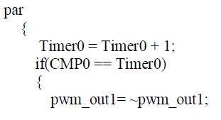
| In implementation timer is realized with desired width and it count is continuously and concurrently compared with other compare registers with digital comparators. When data is matched output pin state is changed accordingly. The following code realizes the actual implementation of the DAC. |
 |
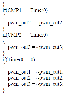 |
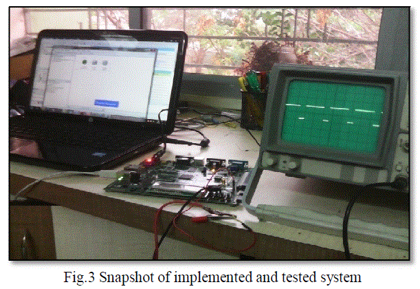
| The code inside the par statement executes concurrently generating parallel operating hardware with comparing compare register 0,1,2 simultaneously with Timer and generate PWM, when compare match occurs. Handel C provides many output file formats like VHDL, VERILOG, and EDIF. Here intermediate format EDIF is generated and used for further synthesis, place and route. This EDIF format is intermediate format which is platform and tool independent which can be used with any tool and any platform. EDIF files are synthesized in XILINX ISE ver12.4. After that Bit file is generated and programmed into SPARTEN 3E FPGA and result is tested. Figure 3 shows the implemented and tested system output. |
 |
| The produced output PWM should be filtered through low pass filter to remove high frequency switching content to produce desired analog output. This filtering can be done with simple RC filter. For analog output required minimum filter cutoff frequency is given by; |
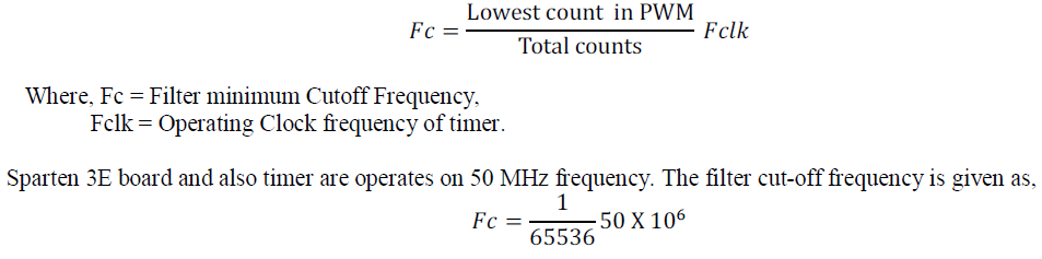 |
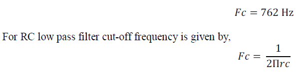 |
| But these simple directly connected RC filters have drawbacks that there output impedance places limitations when interfacing with external circuitry. Also they have very low output driving capability. In many cases simple RC filter is not sufficient for filtering. |
| To avoid these problem two pole active sallen key low pass filter is implemented. Sallen key has non inverting configuration, High input impedance, and low output impedance with near about -40db attenuation in stop band. The implementation of this filter is shown in fig 4. |
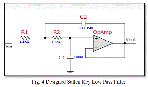 |
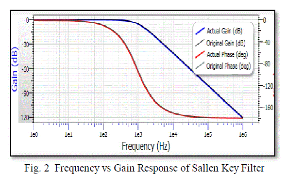
| This topology have benefit that its gain can be changed without affecting filtering components. Here gain is set to unity. The below fig 5. reveals the frequency vs gain response of Sallen Key filter. |
 |
CONCLUSIONS |
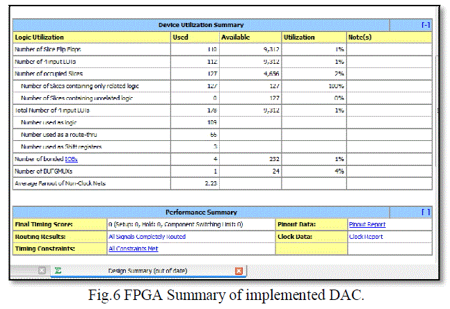
| FPGA based 3 channels concurrent DAC has designed and tested successfully. It requires 2638 NAND gates for implementation of 115 flip flops, utilizing 178 LUTs which is near about 1% utilization of total resources. The following FPGA summary gives details about it. |
 |
| It can be concluded that mixed signal systems can achieve maximum benefits than just single analog or digital one. As per the system design requirement, we configured the resolution of the DAC and can achieve the maximum efficiency. The designed soft IP core also reduces the time to market term at instant of system design which is very much important issue in industry for the competitive success. As FPGA are well established for system on chip design, the reconfigurable soft IP core for high-resolution DAC is flexible and cost-efficient solution for FPGA based designs. |
ACKNOWLEDGMENTS |
| The First author thankful to UGC for Meritorious Fellowship and Remaining Authors grateful to UGC for UGC major research project “Development, Testing and prototyping of wireless sensor network for earthquake early warning system” for support and finance assistance. |
References |
|