International Journal of Advanced Research in Electrical, Electronics and Instrumentation Engineering
ISSN ONLINE(2278-8875) PRINT (2320-3765)
ISSN ONLINE(2278-8875) PRINT (2320-3765)
Nisha John1 and Prof. Sadanandan G.K2
|
| Related article at Pubmed, Scholar Google |
Visit for more related articles at International Journal of Advanced Research in Electrical, Electronics and Instrumentation Engineering
Several new generation wideband data communication systems nowadays, have adopted Orthogonal Frequency division Multiplexing technique. FFT/IFFT is one of the main kernel in the OFDM system, therefore, special attention needs to be given to optimize the FFT block. Hence, utilizing low power, area efficient as well as high speed multipliers and adders in Fast Fourier Transform will ensure enhanced performance and efficiency. Urdhva Tiryakbhyam is one of the age-old Indian Vedic sutra dealing with multiplication which enables parallel generation of partial products and completely eliminates unwanted multiplication steps. Multipliers implemented using Vedic mathematics are superior in terms of area efficiency. Carry Select Adders (CSLA) are one of the fastest adders used in several processors to perform fast and complex arithmetic functions. In this work, the vedic multiplier which is developed using the Urdhva Tiryakbayam Sutra along with modified carry select adder is used to perform a Radix-22 pipeline Fast Fourier Transform. The Fast Fourier Transform (FFT) which is implemented using vedic multiplier and modified adder is then compared with FFT implemented using traditional multipliers and adders and its performance is verified. Such an FFT will be most suitable to OFDM communication system. The coding of the FFT processor developed based on vedic mathematics is done in VHDL (very high speed integrated circuit hardware description language) and synthesis is done using Xilinx ISE series.
Keywords |
| Radix 22 FFT ,Algorithm ,OFDM, Urdhava Tiryakbhyam, CSLA. |
INTRODUCTION |
| OFDM transmissions are emerging as a predominant multi- carrier modulation technique because of its capability of ensuring high level robustness against interference. OFDM modulation technique is now extensively used in numerous high speed mobile and wireless communication systems as; fixed Wi-Fi system ,fixed WiMAX system (IEEE 802.16a standard), Asymmetric digital subscriber line (ADSL), mobile WiMAX system (IEEE 802.16e standard) and Wireless Local Area Network (WLAN). It provides high bandwidth efficiency because the carriers are orthogonal to each other and multiple carriers share the data among themselves. Fast Fourier Transform (FFT) is one of the key components in an OFDM system. Nowadays, several communication systems require higher points FFT and higher symbol rates. This requirement establishes challenges for low power and high speed FFT designs with large number of points. |
| The FFT algorithm eliminates the redundant calculation which is needed in computing Discrete Fourier Transform (DFT) and is thus very suitable for efficient hardware implementation [13]. In addition to computing efficient DFT, the FFT is the core processing block in several widely used applications such as linear filtering, digital spectral analysis, image processing and correlation analysis .One of the major concerns for researchers is to meet this real-time processing requirement and to reduce the hardware complexity mainly with respect to area and power and to improve processing speed over the last decades. Hence, designing a pipeline FFT processor would provide optimum solution for speed, but it occupies more area for different stages used in the pipeline and also increase the implementation complexity. Thus, utilizing a novel structure suitable for FPGA implementation along with reduced complexity of the FFT processor is necessary to ensure enhanced computational efficiency and improved performance. An efficient hardware oriented radix-22 algorithm is developed by integrating a twiddle factor decomposition technique. This is done by divide and conquer approach to form a spatially regular Signal Flow Graph (SFG). Mapping the proposed algorithm to the cascading delay feedback structure leads to the proposed architecture [11]. Vedic Mathematics is the ancient system of mathematics which has unique techniques of calculations based on 16 Sutras .All the Vedic formulae are claimed to be based on the natural principles on which the human mind works. The paper utilizes “Urdhva Tiryakbhyam” algorithm of ancient Indian Vedic Mathematics which is utilized for multiplication in complex twiddle multipliers. The next sections describes about the literature reviewed. The algorithms & also the design methodology towards developing an efficient FFT Core utilizing vedic mathematics which is aimed at increasing the performance of the an OFDM system. Finally, we conclude with a comparison of the hardware requirement of our proposed FFT with conventional FFT. |
LITERATURE REVIEW |
| Satyendra Sharma and Unnati.C.Mehta in 2011 [17] presented a straightforward approach for pipeline implementation of radix-2 FFT algorithm called as Radix-2 single-path Delay Commutator (R2SDF) along with FIFO design for Mobile Wi-MAX. It was observed that at different stages of the design, the requirement of FIFO was different. The length of the FIFO depended on which stage of pipeline it was used. Width of the FIFO depends upon the word length used ,this led to increased width for higher word length. The input sequence was broken into two parallel data stream flowing forward, with correct “distance” between data elements entering the butterfly scheduled by proper delays. This architecture required log2 N radix-2 butterflies, as well as Log2 N-2 multipliers which was considered as the disadvantage of this architecture. |
| Bin Zhou , David Hwang and Yingning Peng in 2007[4] noticed most of the works related to Radix-4 Single-path Delay Commutator (R4SDC) and proposed an area-efficient algorithm. The R4SDC which was a Radix-4 version of Radix-2 Single-path Delay Feedback, employed CORDIC iterations for the pipelined processing of fast fourier transform. A single data stream goes through the multiplier at every stage. The utilization of multipliers was increased to 75% due to the storage of three out of radix-4 butterfly outputs. The utilization of the radix-4 butterfly was fairly complicated and contained at least 8 complex adders, hence it resulted in a very complex implementation of the processing elements (PEs). This design involved complex controller design which created a long critical path. It required log4 N -1 multipliers, log4 N full radix-4 butterflies and storage of size N – 1. Such an architecture provided a lesser throughput per area. |
| Marti-Puig, Reig Bolano in 2009[14] derived two families of radix-4 factorizations for the FFT that have the property that both inputs and outputs are addressed in natural order. These families were obtained from another two families of radix-2 algorithms that have the same property. The algorithms obtained had the same number of multiplications and additions (mathematical complexity)as that of Radix-4 Cooley-Tukey algorithms but eliminated the input or output bit-reversal ordering applied in Cooley-Tukey algorithm. The hardware realization of Radix 4-FFT was done by multi-bank memory along with "in place" addressing strategy which reduces the memory access time and minimizes the hardware consumption. The main drawback was that, it suffered from low utilization of all components, which could be compensated only in certain special applications. |
| Angel M. Burón ,Gustavo Ruiz ,Jesús García and Juan A. Michell in 2007[3] explained the realization of a Split Radix FFT (SRFFT) processor based on a pipeline architecture for signal and image processing application. This architecture focused on combining the higher parallelism of the Radix-4 FFTs and the possibility of processing sequences having length of any power of two. This architecture has as its basic building blocks a Complex Butterfly and a Delay Commutator. But the delay commutator had to be designed to be customized for even and odd SRFFT computation levels. The main drawback was the irregular structure compared to mixed radix and constant radix algorithms. Because of the irregular structure, this algorithm was not suitable for parameterization. It was most used with segmented arithmetic of any level of pipeline in order to speed up the operating frequency. |
RADIX-22DECIMATION IN FREQUENCY FFT ALGORITHM |
| Related works done indicated that one of the most efficient architecture in terms of memory utilization was the delay feedback Radix-4 algorithm based single-path architectures, but they required higher multiplier utilization; however, the Radix-2 algorithm based architectures have simpler butterflies and control logic. The Radix-22 algorithm used in the FFT design has the advantage that it retains the Radix-2 butterfly structures but has the same multiplicative complexity as Radix-4 algorithms. This makes the R22 SDF FFT algorithm an excellent choice for the VLSI implementation. An informative state-of-the-art review of hardware architectures for FFTs was given by He et al. [14] and different approaches were put into functional blocks with unified terminology. From the definition of DFT of size N [5]: |
 |
| Start by classical divide-and-conquer Radix-2 DIF indexing: |
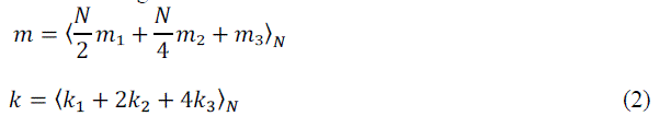 |
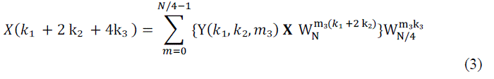
| On substituting (1) in (2),also by applying Common factor algorithm (CFA) a set of 4 DFTs of length N/4is derived as, |
 |
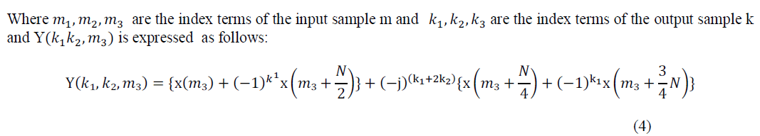 |
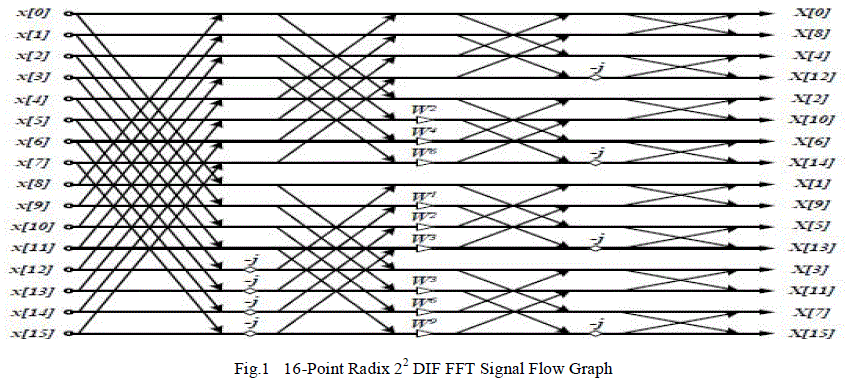
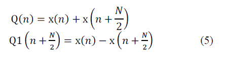
| The previous equation (4) represents the first two stages of butterflies with only trivial multiplications in the Signal Flow Graph (SFG), as Butterfly I (BFI) and Butterfly II (BFII). Complex full multipliers are required after the two butterflies in order to compute decomposed twiddle WNm3(k1 + 2 k2) .The order of the twiddle factors in the radix 22 algorithm is different from that of radix-4 algorithm. By applying the common factor algorithm recursively to the remaining DFTs of length N/4, the complete radix-22 FFT algorithm is derived. The corresponding FFT signal flow graph for N=16 is shown in Figure 2, where trivial multiplication by - j, represented by the small circles in the figure below, involves only real-imaginary swapping and sign inversion. The multiplicative operations are in such an arrangement that only every other stage has non-trivial multiplications. When pipeline/cascade FFT architecture is under consideration, this multiplicative arrangement provides a great structural advantage over several other algorithms. |
 |
PROPOSED METHOD |
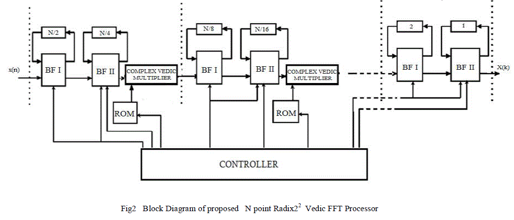
| In the proposed FFT architecture, Radix-22 DIF FFT algorithm derived in the previous section is mapped to the radix-2 Single delay feedback(SDF) architecture, and a new Radix 22 SDF architecture approach is obtained. Fig 2 outlines an implementation of the proposed architecture for N=64, the similarity of the data-path to R2SDF and the reduced number of multipliers within the architecture can be noted. The implementation uses two kinds of butterflies; one identical to that in Radix2 SDF architecture, while the other also contains the logic to implement trivial twiddle factor multiplication, as shown below in Fig 3 and Fig 4 respectively.The proposed 64-point Radix- 22 fixed-point FFT consists of six Radix-2 butterflies designed using modified adders, feedback registers along with each butterfly, two complex vedic multipliers, two twiddle factor rom, and a controller module that provides the control signals to each of the butterflies. The feedback registers vary in length from 1 to 32-bits and are indicated below accordingly in the fig2.The twiddle values are generated by a Matlab program and the twiddle values are converted to fixed point and stored in the rom. Due to the spatial regularity of Radix-22 algorithm, the controller module of the processor is very simple. It serves two purposes: address counter for twiddle factor reading in each stage and also as a synchronization controller. |
 |
| A.Butterfly Structures |
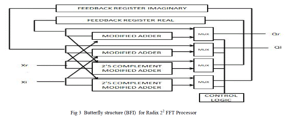
| The scheduled operation of the pipelined Radix 22 Single- path delay feedback FFT processor in Fig 3 can be explained with the help of the butterfly structures shown below is as follows. Fig. 3 shows the Butterfly I structure(BF I), the inputs Xr, Xi of this butterfly comes from the FFT input data and in the succeeding stages this input comes from the previous component which is the twiddle factor multiplier. The output data Qr, Qi goes to the next stage which is normally the Butterfly II. The control signal (CNT1) has two options : when CNT1=0, the multiplexers direct the input data to the feedback registers until they are filled in the initial N/2 cycles. The other option is CNT1=1,in the next N/2 cycles, the multiplexers select the output of the adders and subtractors which is implemented by 2’s complement modified adder in the proposed design. This is the butterfly output i.e a 2-point DFT computation with the incoming data and the data stored in the feedback registers. |
 |
| The butterfly outputs Q(n) and Q1(n + N/2) are computed according to the equations given in eqn (5). Q(n) is sent to the next stage and Q1(n + N/2) is sent back to the feedback registers to be “multiplied” in the next N/2 cycles when the first half of the next frame of time sequence is loaded in. Operation of the second butterfly (BF II) is similar to that of the first one(BF I), except the “distance” of butterfly input sequence are just N/4. After N-1 clock cycles, the result of the complete DFT transform streams out to the last BFII structure. The next frame of transform can be computed continuously without pausing due to the pipelined processing of each stage. |
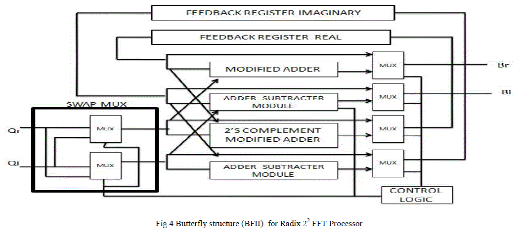
| The input data Qr, Qi comes from the previous component, Butterfly I. The output data from the Butterfly II are Yr, Yi, as well as the real and imaginary feedback signals. Feedback signals are fed to the next component, that is the twiddle factor multiplier. The multiplication by –j involves swapping between real part and imaginary part and sign inversion. Swap-MUX efficiently handles the swapping and the sign inversion is handled by switching between the adding and the subtracting operations performed by the adder/subtractor module. The control logic is activated when there is a need for multiplication by −j, therefore the real and imaginary data will swap and the adding and subtracting operations will be switched. Rounding off has been also applied to reduce the scaling error. |
 |
 |
| B. Complex Multiplier Design Employing Vedic Concepts |
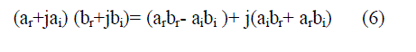
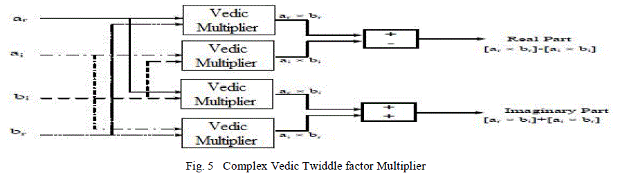
| Multiplication operation is regarded as one of the most important function in several signal processing systems, but is a very complicated and expensive one. The complex multiplier is used in the algorithm for multiplying the twiddle factor stored in ROM (ar+jai) by BFII output (br+jbi) which is expressed in the equation below can be realized by Vedic multipliers, adder and subtractor. This complex multiplier structure occupies large chip area in VLSI implementation, but introducing vedic technique have helped in reducing the size and also improving the speed of multipliers. |
 |
 |
| Urdhva Tiryakbhyam sutra which implies Vertically and Crosswise, an interesting Indian Vedic Sutra is utilized for the multiplication in the FFT processor. This technique is explained as follows: consider 2 decimal numbers initially, the same concept is applied to binary numbers. Let the decimal numbers be A and B where A = p1p0 and B = q1q0. Firstly, the least significant bits of the numbers are multiplied which gives the least significant bit of the final product(s0) i.e vertical as the sutra specifies. Then, as the next step the LSB of the multiplier is multiplied with the next higher bit of the multiplicand and is added with the product of LSB of multiplicand and next higher bit of the multiplier i.e crosswise as the sutra suggests. The sum gives the second bit of the final product(s1) and the carry(c1) is added with the partial product which is obtained by multiplying the most significant bits to give the sum and carry bits. The sum is the third corresponding bit(s2) and the carry (c2)becomes the fourth bit of the final product. The final result (c2s2s1s0) is obtained by combining the three steps mentioned above. |
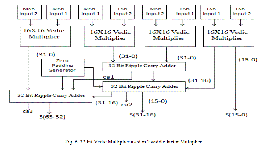
| Urdhava employs a novel concept in which all partial products are calculated in parallel and the delay is only due to the time taken for the carry to propagate through the adders. The 2X2 Vedic multiplier module is implemented using four input AND gates & two half-adders. The implementation of 4x4 bit Vedic multiplier uses the 2x2 bit multiplier as a basic building block. The same method is extended for input bits 8, 16 & 32.The architectural design of the 32 bit vedic multiplier employed in the complex multiplier using 16X16 bit multiplier as a basic building block is shown below. The main advantage of the Vedic Multiplication algorithm (Urdhava Tiryakbhyam Sutra) stems from the fact that it can be very easily implemented in FPGA due to its regularity and simplicity. |
 |
| C. Modified adder |
| Carry Select Adders (CSLA) is used widely in many computational system designs to ensure area- and powerefficient high-speed data path. Such adders moderate the existing problem of carry propagation delay by independently generating multiple carries, then selecting a carry to generate the sum. In this paper, we have designed the modified CSLA to be employed within the butterfly structures of the FFT core. Regular CSLA uses independent sets of ripple carry adders (for Cin=0 and Cin=1) to generate the resultant sum. Then, the final sum and carry are selected by the multiplexers. Ripple-carry adder allows for fast design time as the layout of the structure is simple. However, since each full adder must wait for the carry bit to be calculated from the previous full adder, the ripple-carry adders are relatively slow. Hence, from this it is evident that the Regular CSLA is not area and speed efficient because it uses multiple pairs of Ripple Carry Adders (RCA) which leads to increased delay.To overcome the problem mentioned above, the basic idea of the proposed work is to use n-bit binary to excess-1 code converters (BEC) and carry look ahead logic to improve the speed of addition as well to make the structure area efficient. The BEC logic can be used to replace the RCA for Cin=1 in the regular CSLA as it performs the same function using the lesser number of logic gates than RCA for Cin=1. Using carry look ahead logic instead of RCA for Cin=0 in the regular CSLA will achieve lesser delay and accelerate the addition operation. |
SIMULATION AND IMPLEMENTATION RESULTS |
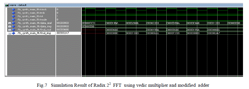
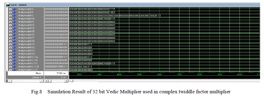
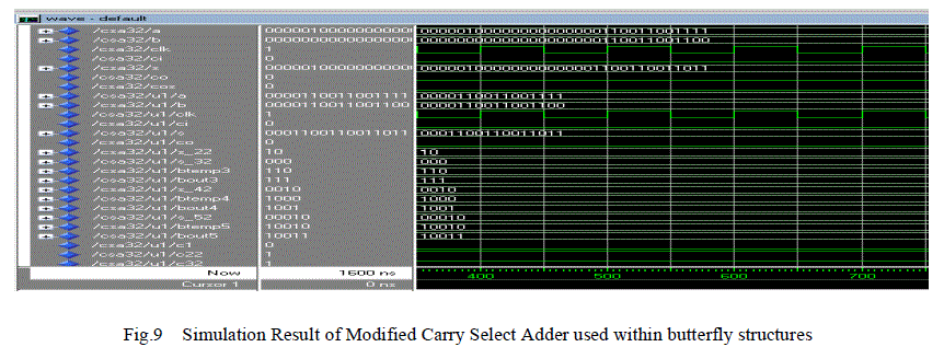
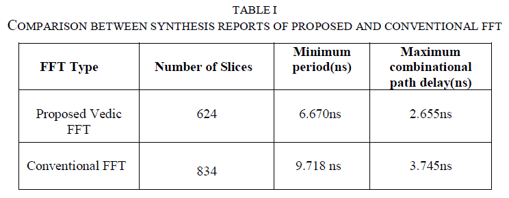
| An efficient 64 point Radix-22 FFT module was designed using Vedic multipliers and modified adder and simulated using VHDL.FFT utilizing modified wallace multiplier and regular carry select adder was also simulated to compare the performances in terms of area and speed. Both the designs were implemented using the Sparten 3E and their synthesis reports were analysed. Fig 7 shows the simulation of the testbench which was developed to test and verify the 64 point FFT. The values were verified with Matlab output. Fig 8&9 show the simulation of the complex vedic multiplier and the modified adders utilised in the proposed processor. The 32 bit inputs are entered in both cases and the product and sum is verified respectively. The conclusion prove that our proposed system is better in terms of area and speed compared to the existing FFT processors. |
 |
 |
 |
 |
CONCLUSION |
| In this paper, Vedic FFT processor with Radix 22 FFT algorithm is designed and implemented using Sparten 3E FPGA and is attractive to be used in real-time systems .Implementation results prove that the proposed FFT led to 26% area reduction and 29% speed improvement when compared with conventional FFT. This design had a maximum clock frequency of 95.2MHz. Such a 64-point FFT implemented using vedic concepts and modified adder was found to have a good balance between performance and hardware requirements and is therefore most suitable for use in OFDM. The results are a clear indication that the processing time of the proposed FFT is below the OFDM symbol period of 4μsec, which ensures an appropriate operation for the communication standard application requirements of mobile WLAN(IEEE 802.11a), which uses OFDM modulated wireless communication system. |
References |
|