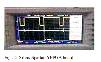
In this paper, the design and analysis of an experimental study of on FPGA controlled quasi-double boost converter is presented. The study also aims to enhance undergraduate’s knowledge on experimental studies in the laboratory. The performance of FPGA based quasi double boost converter design is analysed through the simulation under various duty cycle and compared with simple boost converter. The results are validated through the experimental setup based on Xilinx Spartan 6 FPGA board with Xilinx 12.1 and ULK control panel.
Keywords |
| FPGA, Quasi-Double Boost Converter, Simulation, VHDL, FUZZY Logic. |
INTRODUCTION |
| High step-up converter suits the many emerging applications in power generation via fuel cell, PV cell arrays and wind
power [1] as well as other industries like automotive, IT and communications. When it is required to connect the low
voltage source to a relatively high voltage load or power grid, basic boost topologies [2] do not provide sufficient boost
factor. There are many proposed topologies such as tapped –inductor boost, double cascade boost, intervaled boost and
assymetric boost converter [3]-[4]. There are different control methods to adjust the duty cycle of dc to dc converters
such as PID controllers, sliding mode controllers [5] and intelligent control methods like fuzzy control [6]. |
| Due to non linear behaviour of dc to dc converters, conventional controllers like PID are difficult to tune. Fuzzy logic
finds its application in such type of control system because it does not require the exact model of plant/process. Fuzzy
works on the operator experience and linguistic control laws are implemented. |
| Implementation of Fuzzy, Digital PI or PID controllers using microprocessor, microcontroller and DSO is more
popular but computing speed limits the use of these digital implementation. The new generation of applications
requires more flexible and higher performance without increasing cost and resources. Two approaches are there to
implement digital controller: sequentional and concorent .The sequential task execution takes longer processing time to
accomplish the same task (up, uc and DSP).The concorent base or hardware based like FPGA are becoming alternative
solution for the realization of digital control systems [9]-[10].HDL language (VHDL/Verilog) is used to program the
FPGA [12]-[13].The MOSFET switches of dc to dc converters are controlled by PWM signal generated by FPGA
board [14]. |
QUASI DOUBLE BOOST CONVERTER |
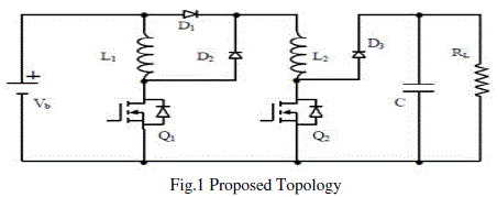
| For many emerging applications, a high boost factor is required. The basic boost topology does not provide a high
boost factor. The proposed topology provides higher boost factor and extending the control range. Fig.1 shows the
proposed topology. It consist of two inductors L1 & L2 having same values , three diodes D1-D3 are of same types
and two switches S1 & S2 having same assumptions. It is similar to paralleling two single/classic Converters. |
 |
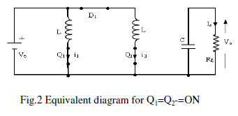
| Equivalent Diagram in ON State: Let us firstly consider ideal components. When the transistors Q1 & Q2 are in ON
state, the proposed topologytransfers energy from the dc source (Vb) into the inductors L1 & L2 as can be seen in Fig.2,
where i1 is the current through inductor/transistor1, i2 is the current through inductor/transistor 2, io is the output current
through load RL and C is the smoothing capacitor. |
 |
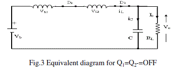 |
| Equivalent Diagram in OFF State: During the OFF state, the two inductors are connected in series, as shown in the
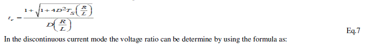
equivalent diagram Fig.3.The converter can work in both continuous current mode or in discontinuous current mode. IM
the maximum current flowing in the inductor can be obtained via expression as |
 |
 |
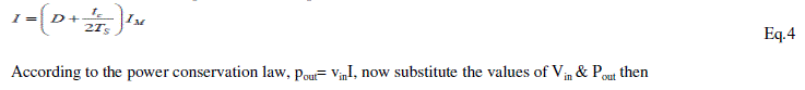
 |
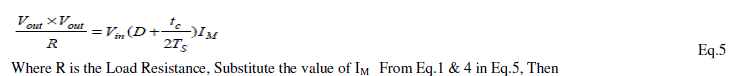
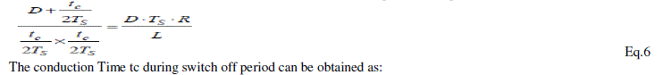
| According to the power conservation law, pout= vinI, now substitute the values of Vin & Pout then |
 |
 |
 |
 |
 |
 |
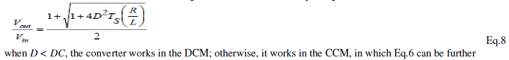
| The boost factor of this converter is equal to (1+D)* boost factor of simple boost factor. For maximum value of D=0.9
M(Double Boost)= 1.9*M(simple Boost). It is not exactly double the boost factor of simple boost that’s why called
quasi double boost converter. |
 |
FUZZY CONTROL SYSTEM |
| 3.1 Fuzzy Logic Controller :Traditionally, PI, PD and PID controller are most popular controllers and widely used in
most power electronic closed loop appliances however recently there are many researchers reported successfully
adopted Fuzzy Logic Controller (FLC) to become one of intelligent controllers to their appliances with respect to their
successful methodology implementation. |
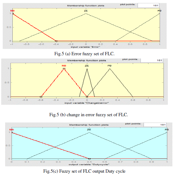
| FLC using in this paper has two inputs which are: error and the change in error, and one output feeding to the DC to
DC converter. |
| FLC contains three basic parts: Fuzzification, Base rule, and Defuzzification. |
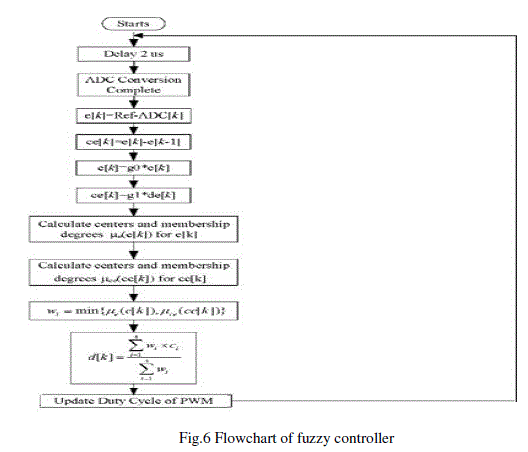
| Fuzzification :Fig.5(a) - (c) illustrates the fuzzy set of the inputs Error & Change in error and output Duty cycle
which contains 3 Triangular memberships functions. |
 |
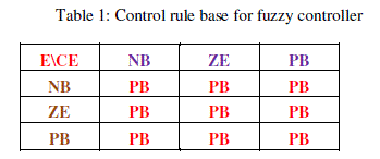
| Control rule base:The knowledge base defining the rules for the desired relationship between the input and output
variables in terms of the membership functions illustrated in Table1 |
 |
| Defuzzification:There are two widely used approaches in FLC implementation: Mamdani and Sugeno. In this paper,
Mamdani approach has been used to implement FLC. The centre of gravity method is widely used in Mamdani
approach which has been selected in this paper to compute the output of the FLC.The flow chart of FLC is shown in
Fig.6 |
 |
FUZZY CONTROLLER IMPLEMENTATION ON FPGA |
| Implementation of fuzzy controllers on the FPGA had quite different issues from implementation of linear controllers.
The implementation of linear controllers usually involves difference equations, which are linear combination of
feedback and control signals. The FLC is implemented on the same FPGA board using Xilinx_ISE 12.1 software. The
inputs of the controller are the error and change in error, the output of the controller is connected with a PWM module
designed on the FPGA. The PWM frequency of the modulating signal is about 3 KHz, this value calculated by
experiment. A 14-bit counter runs at the clock of FPGA =50MHz completes cycles at a rate 50M/214 ≈ 3 KHz. In this
case, each level in an 8-bit modulating signal corresponds to 214/256 = 26 clock pulses.Here we used Mission 10x-
Unified Learning Kit R3.0 which include Spartan-6 FPGA XC6SLX25T FPGA and on board 10-bit, 20MSPS
sampling analog to digital converter (ADC)AD9200 from Analog devices. |
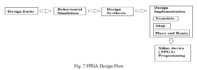
| FPGA Design Flow:Fig.7 shows the sequence of steps followed when implementing PWM Generator design on
FPGA. |
 |
| These steps are discussed here as: |
| 4.1 Design Entry:This is the first step of implementing a design on FPGA. In this step the VHDL (Very High Speed
Integrated Chip Hardware Description Language) code of ADC Block, FUZZY Block and PWM Generator block is
written using software Xilinx ISE 12.1. Structural modeling was used for writing the code. After writing the code
syntax check was performed on the code to see whether code was properly written using correct syntax. |
| 4.2 Behavioral Simulation :The next step is behavioral simulation. This step verifies whether the design entered is
functionally correct or not. This simulation is called RTL simulation. For this simulation VHDL Test bench was written
for PWM Generator architecture and simulation was seen in Xilinx ISE Simulator. After it is verified it is functionally
correct we move onto next step. |
| 4.3 Design Synthesis :The VHDL code of PWM Generator is then synthesized using Xilinx XST which is a part of
Xilinx ISE software. There is an option of Synthesis in process tab of Xilinx ISE which performs the operation of
synthesis .The synthesis process is used for optimizing the design architecture selected. The resulting netlist is saved to
an NGC file. After design synthesis, synthesis report is generated which gives information about how many logic
blocks are used and what is the device utilization of the design architecture synthesized. Synthesis basically maps the
behavioral design to gate level design. |
| 4.4 Design Implementation :After design synthesis, design implementation is done which comprises of following
three steps |
| (a) Translate |
| (b) Map |
| (c) Place and Route |
| Before translating the design, User Constrained file (UCF) is written to assign pin configuration of the FPGA to the all
blocks I/O’s. Once this is done Translate merges together this UCF file and netlist generated after synthesis into Xilinx
design file Mapping is done to fit the design into the available resources of target device i.e. FPGA. This is also
important step of design. Last step of Design Implementation is Placing and Routing which places the logic blocks of
the design into FPGA and route them together so that they occupy minimum area and meet timing requirements. This
operation produces NCD output file. |
| 4.5 Xilinx Device (FPGA) Programming :There is a option of Generate programming file on the process tab of Xilinx
ISE which converts the NCD file generated after routing to BIT file. It produces a bit stream for Xilinx Device (FPGA
in this case) configuration. This BIT file is used to create xsvf file to program the FPGA. |
| 4.6 Configuring Target Device :There is option of Generate Target PROM/ACE on the process tab of Xilinx ISE
which converts the BIT file to the PROM or ACE file. This PROM or xsvf file can be downloaded directly into the
FPGA’s memory cells. We have to make sure that FPGA is connected to the PC where we are developing this design.
After we download xsvf file into the FPGA the FPGA is ready to be used as Fuzzy logic controller. The out pin is
connected to the driver of the MOSFET’s. |
VHDL CODING OF FUZZY LOGIC |
| 5.1 Fuzzyfication:Each trapezoidal membership function is defined by two points and two slope values. The entire
membership function can be divided into three segments: 0, 1 and 2 as shown in Figure 1.The Y axis shows the degree
of membership (μ) as a value between 0 and 1. The X axis shows the universe of discourse and is divided into three
segments. The degree of membership depends on the location of the input value with reference to these three segments. |
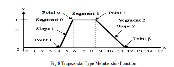 |
| Fig.8 shows how trapezoidal input membership functions are formed in the Fuzzification process. The calculation of
the degree of membership ((μ) can be categorized into three different segments: |
| (a) in segment 0: μ = 0, |
| (b) in segment 1: slope is upward from left to right, therefore: |
| μ = (Input value – point 1) * slope1, |
| where μ is limited to a maximum value of 1 |
| (C) in segment 2: slope is downward from left to right, therefore: |
| μ = 1 - (Input value –point 2) * slope 2, |
| where μ is limited to a minimum value of 0.As an example, let’s use the input value of 10 to calculate the degree of
membership function. Using an 8-bit resolution computation, μ = 1 equals to $FF or 255 in decimal (the “$” sign
indicates hexadecimal number representation). The values of Point 1 and Point 2 are $04 and $09, respectively, and the
two slopes can be calculated as follows: |
| Slope 1 = 1 / (6 – 4) = $FF / 2 = 255 / 2 = 127 = $7F (1) |
| Slope 2 = 1 / (12 – 9) = $FF / 3 = 255 / 3 = 85 = $55 (2) |
| Since the input value of 10 ($0A) is greater than Point 2 and lies in segment 2,therefore , |
| $FF – (Input value – point 2) * slope 2 = $FF – ($0A - $09)*$55 = $AA (3) |
| In VHDL, each membership function is defined by four 8-bit values, two points and two slope values using record type
declaration as follow: |
| type membership is (term, none); |
| type mfs is record |
| linguistic: membership; |
| point1: std_logic_vector(7 downto 0); |
| slope1: std_logic_vector(7 downto 0); |
| point2: std_logic_vector(7 downto 0); |
| slope2: std_logic_vector(7 downto 0); end record; |
| type membership_functions is array(natural range <>) mfs; |
| constant linguistic_name : membership_functions :=((linguistic => term, point1 => x"04", |
| slope1 => x"7F", point2 => x"09", slope2 => "55"), linguistic => none, point1 => x"FF", |
| slope1 => x"FF", point2 => x"FF", slope2 => x"FF")); |
| 5.2 Rule Evalution:A rule usually takes the form of IF-THEN statement as follow: |
| IF x is A AND y is B THEN z is C
“AND” is a fuzzy operator which is the minimum operation between the two antecedents. InVHDL, the following
“minimum” function is used to obtain the result of each rule evaluation between two variables: |
| function minimum(a, b: std_logic_vector) return std_logic_vector is |
| variable min: std_logic_vector(7 downto 0) := (others => '0');begin |
| if a < b then min := a; else min := b; end if; return min; end minimum; |
| There is also an implied “OR” operation between successive rules when more than one rule is involved with the same
output. The linguistic rule, IF (x1 is A1 AND y1 is B1) OR (x2 is A2 AND y2 is B2) THEN z is C, can be implemented
by taking the maximum value of all the results with the same consequent block. In VHDL code, a function of taking the
maximum of two input variables to determine the final result of all rules with the same output can be written as: |
| function maximum(a, b: std_logic_vector) return std_logic_vector is |
| variable max: std_logic_vector(7 downto 0) := (others => '0'); begin |
| if a > b then max := a; else max := b; end if; return max; end maximum; |
| By combining the “minimum” and “maximum’ functions, the truth value for each rule can be
obtained as: |
| C <= maximum( minimum(A1, B1), minimum(A2, B2)); |
| 5.3 Defuzzyfication:During the Defuzzification process, each fuzzy output is multiplied by its corresponding singleton
position. The sum of this product is divided by the sum of all fuzzy output to obtain the result of the final output. In
VHDL, this is implemented as: |
| For i = 1 to n do begin product = (s(i) × f(i)) + product; sum = f[i] + sum; end for loop; |
| output = product / sum; |
PWM SIGNAL GENERATION |
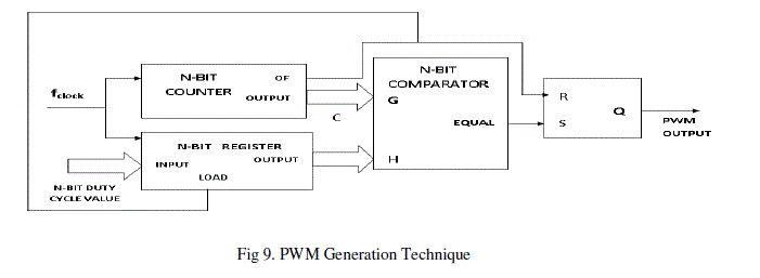
| This architecture is a high speed N-bit free running counter whose output is compared with register output; which
stores desired input duty cycle( N-bit value); with the help of comparator. The comparator output is set equal to 1 when
both these values are equal. This comparator output is used to set RS latch .The overflow signal from counter is used to
reset RS latch. The output of RS latch gives the desired PWM output.. This overflow signal is also used to load new Nbit
duty cycle in Register. The advantage of these method is that it is used to generate High-frequency PWM output
which is not possible in normal counter based approach. Fig,10 shows the corresponding block diagram of this
architecture. |
 |
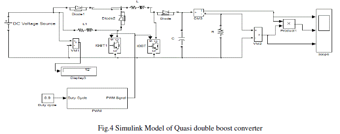
SIMULINK MODEL AND BLOCK DIAGRAM OF PROPOSED SYSTEM |
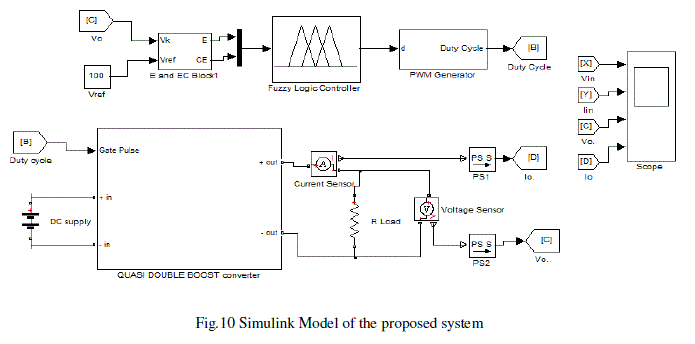 |
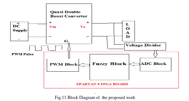 |
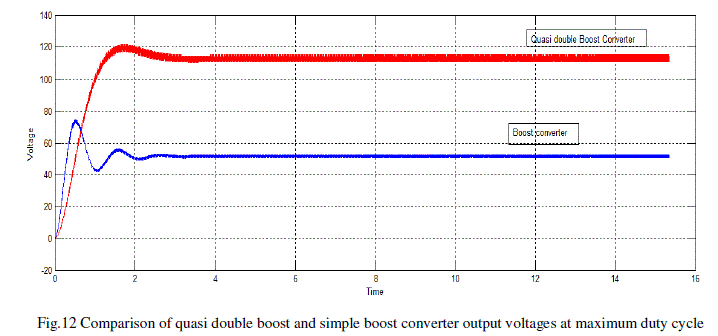
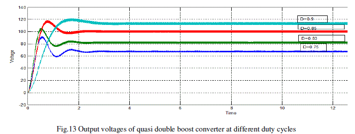
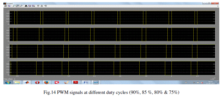
RESULTS AND DISCUSSION |
| Simulation results are obtained from the MATLAB/SIMULINK. |
 |
 |
 |
 |
 |
 |
 |
CONCLUSIONS |
| This paper present the analysis and design of a fuzzy controlled quasi double boost converter to develop
more theoretical and practical knowledge for undergraduates and research scholars on FPGA based control
applications. The basic of software optimization for this converter has been presented in detail. The
simulation results on MATLAB/SIMULINK and XILINX 12.1 are presented for quasi double boost
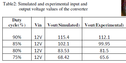
converter.The experimental results show an improvement boost factor. |
References |
- Christopher Lohmeier, JianwuZeng,WeiQiao, LiyanQu, and Jerry Hudgins, âÃâ¬ÃÅ A Current-Sensorless MPPT Quasi-Double-Boost Converter for PV SystemsâÃâ¬ÃÂ, pp 1069-1075,2011 IEEE.
- AthimulamKalirasu and SubharensuSekar Dash, âÃâ¬ÃÅSimulation of Closed Loop Controlled Boost Converter for Solar InstallationâÃâ¬ÃÂ, Serbian Journal of Electrical Engineering,Vol. 7, No. 1, May 2010.
- N. Vazquez, L. Estrada, C. Hernandez and E. Rodriguez, âÃâ¬ÃÅTheTapped-Inductor Boost ConverterâÃâ¬ÃÂ, IEEE International Conference on Industrial Electronics (ISIE), 2007.
- B.S. Min, N.J Park and D.S. Hyun, âÃâ¬ÃÅA Novel Current Sharing Technique for Interleaved Boost ConverterâÃâ¬ÃÂ, 38th IEEE Power Electronics Specialists Conference, 2007
- V.S.C.Raviraj, P.C.Sen âÃâ¬ÃÅComparative study of Proportional-Integral, Sliding mode and Fuzzy Logic Controllers for Power ConvertersâÃâ¬ÃÂ, IEEE Trans on Industry Applications, Vol.33, No.2, March/April 1997.
- MitjaTruntic,MiroMilanovic and Zarko Cu-cej, âÃâ¬ÃÅ Implementation of Fuzzy-logic State Controller in FPGA for Step-down Converter âÃâ¬ÃÂ, Proceedings of the 17th World Congress ,the International Federation of Automatic Control Seoul, Korea, July 6-11, 2008.
- Dancy A.P., Amirtharajah R. and Chandrakasan A.P., âÃâ¬ÃÅHigh-Efficiency Multiple-Output DCâÃâ¬ÃâDC Conversion for Low-Voltage SystemsâÃâ¬ÃÂ, IEEE Trans. on Very Large Scale Integration (VLSI) Systems, Vol. 8, No. 3, June 2000: pp.252-263
- Sajina .S1 and P.SujaBanu, âÃâ¬ÃÅ A Novel Control Strategy Based Converter Architecture for Distributed Energy ResourcesâÃâ¬ÃÂ, International Journal of Electrical Engineering. ISSN 0974-2158 Volume 6, Number 4 (2013), pp. 405-416
- SumanthDonthi, and Roger L. Haggard, âÃâ¬ÃÅA survey of Dynamically reconfigurable FPGA devices,âÃâ¬Ã Proceedings of the 35th South eastern Symposium on System Theory, pp. 422 âÃâ¬Ãâ426, 2003.
- R. Ramos, X. Roset, A. Manuel, âÃâ¬ÃÅ Implementation of fuzzy logic controller for DC/DC converters using field programmable gate arrayâÃâ¬ÃÂ, in: Proc. 17th IEEE Instrumentation and Measurement Technology Conference, vol. 1, 2000, pp. 160âÃâ¬Ãâ163.
- Lattice Semiconductor, âÃâ¬ÃÅInterfacing Analog to Digital Converters to FPGAsâÃâ¬Ã A Lattice Semiconductor White Paper October 2007.
- Douglas L. Perry, âÃâ¬ÃÅVHDL: Programming by ExampleâÃâ¬ÃÂ, McGraw-Hill.
- Vijay Polavarapu,âÃâ¬ÃÅDigital Logic And State Machine Design VHDL ProgrammingâÃâ¬ÃÂ, Spring 2013.
- [=Koutroulis E., Dollas A. and Kalaitzakis K., âÃâ¬ÃÅHigh-frequency pulse width modulation implementation using FPGA and CPLD ICsâÃâ¬ÃÂ, Journal of Systems Architecture , Vol.52 (2006): pp. 332âÃâ¬Ãâ344.
- www.xilinx.com/
- www.xilinx.com/products/silicon-devices/fpga/spartan-6/
- www.iwavesystems.com/unified-learning-kit.html
|