This proposal presents the implementation of the transmitter, receiver and the Viterbi decoder compatible for IEEE 802.15.3c transceiver, as a part of wireless High Definition video transceiver to be integrated in an FPGA. These blocks are implemented on SPARTAN-3 FPGA.
Keywords |
| OFDM, HDMI, UEP. |
INTRODUCTION |
| The trend increase in High Definition (HD) video contents motivated the development of wireless technologies capable
of multi-gigabit per second throughput, like Display Port and High-Definition Multimedia Interface (HDMI).As
today consumer electronic users want the flexibility provided by wireless communications, so video transmission is
also pushing the development of high throughput wireless technologies. |
| The industry alliances (ex: Wireless HD, Wireless USB, MB-OFDM, WHDI) and Standardization bodies (ex:
802.15.3c, ECMA-387, 802.11ac, 802.11ad) activities demonstrate the huge interest in wireless video transmission. The
10 GHz and the 60 GHz (nm-wave) band is the choice for doing development efforts in wireless video transmission. |
| In current wireless technologies video need to be compressed at the transmitter and decompressed at the
receiver but compression and decompression time increases the latency and also it degrades the picture quality
at the receiver incurring in problems for multimedia applications. Video streaming is confined between two devices
that employ the same compression technique, these are the problems in current wireless technologies. For emerging
applications such as wireless video networking in the home, that present high sensitivity to latency, new formats are
capable of delivering uncompressed video. |
| The required net bit rate to transmit uncompressed Full HD video (1920×1080 pixels, with 60Hz refresh and 24-bit
color planes) is about 3 Gbps. The 60 GHz unlicensed band, with 9 GHz of bandwidth, is the choice for these multigigabit
throughputs. Standards as ECMA-387, IEEE 802.15.3c and IEEE 802.11ad use this frequency band to
implement very high throughput WPANs (10 m). |
| The AV mode of IEEE 802.15.3c has chosen for FPGA implementation. It is specially designed for uncompressed video
transmission, taking profit of the asymmetry of the video transmission in order to reduce the hardware complexity of the
transceivers. The Unequal Error Protection (UEP) protects differently bits in accordance with their importance. For
instance, MSB (Most Significant Bit). Portions of uncompressed video data are provided with a stronger error protection
than the LSB (Less Significant Bit), because most significant bits of a color pixel have higher impact on the picture
quality than LSB. |
BASEBAND PROCESSING |
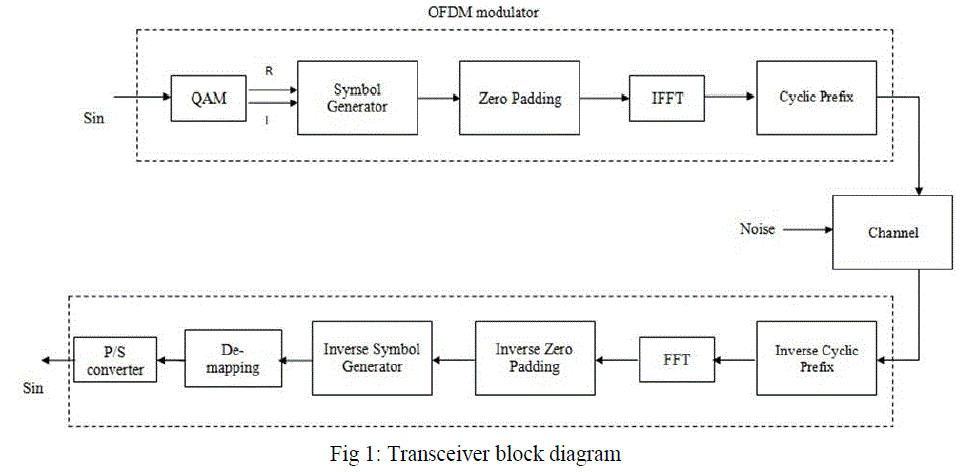
| The transceiver consists of OFDM modulator at the transmitter and OFDM demodulator at the receiver side shown in
Fig 1. We shall first consider the transmitter part. The encoded bits are given to the 16-QAM block, it outputs 16 real
and imaginary values, these values are given to the symbol generator and it generates 64 bit symbol for each real and
imaginary value. Since IFFT to be used is 128-point, so each incoming signal should be 128 bits but output of symbol
generator is 64 bits, so we have to add 32 zero’s on both side and is called zero-padding. Then frequency domain
symbols are converted into time domain using IFFT, and then cyclic prefix is done for each signal and is transmitted
over the noisy channel. The received signal is converted to the frequency domain by the FFT (Fast Fourier Transform)
block. After a de-interleaving process, data carriers are identified and QPSK or QAM symbols are demodulated by the
de-mapper block. The obtained bit stream is de-interleaved and divided into 8 bit streams to be decoded with Viterbi
Decoders (VD). |
 |
| A.IFFT/FFT |
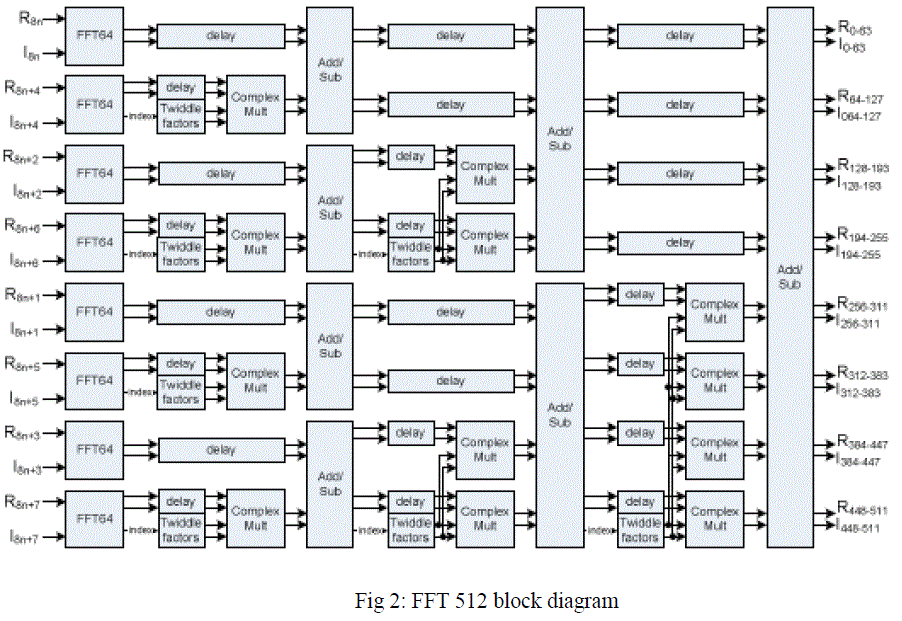
| The OFDM modulator consists of IFFT and demodulator consists of FFT. The FFT/IFFT blocks must process 512
points in 201.73ns. Due to this demanding requirement, the FFT/IFFT implementation is a key block in the transceiver
design. A 512-point FFT Pipeline, Streaming I/O generated by the Xilinx FFT IP core takes 1.18 us to process. So, it
has to be parallelized. We parallelized the FFT calculation, decomposing the 512-point input into eight smaller
sequences. A similar approach was adopted in [4] to implement a 128-point FFT. Each sequence is processed by a 64-
point FFT block pipelined streaming I/O. The outputs of the FFTs are then combined with three-levels of radix-2
butterflies to obtain the final data in eight parallel streams. The implementation adopts full-precision unscaled fixed
point arithmetic, with 11 bit input (3 bits for integer part and 8 for fractional part) and 21 bits output, based on our
modelsim simulations (assuming a coding loss of 0.2 db is acceptable). |
 |
| B. VITERBI DECODER |
| The output of OFDM demodulator is fed to viterbi decoder. The convolutional code has a code rate of 1/3 defined by
the polynomial generators g0 = 133O, g1 = 171O and g2 = 165O. So, the VD generates one bit for each three soft bits.
The Viterbi decoder finds the path in the trellis diagram whose sequence of output symbols best matches the receive
sequence. Its functionality is implemented by four functional units: the branch metric unit (BMU), the add-compare
select unit (ACSU), the survivor memory unit (SMU) and the decision unit (DU). The BMU calculates the distance
(metric) between the received noisy symbol and the output symbol of the state transition (branch). The ACSU
computes the accumulated metric associated with the sequence of transitions (path) to reach a state. The SMU stores
the information that permits to traceback from a state to the previous one Traceback processing is managed by the
decision unit (DU). To guarantee a data rate of at least 3.2 Gbps, each of the VD must work at 400MHz. To achieve
such high data rates in an FPGA, we have adopted the sliding-block method. The sliding block technique permits to use
independent VD to decode a single bit stream. To guarantee correct initial and final states, the method considers an
initial synchronization block and a final trace-back block without decoding for each parallel VD. |
RESULTS |
| The transceiver architecture was implemented using Verilog hardware description language. These descriptions were
then processed by standard Xilinx ISE 12.2 design tool suite, which performed synthesis, placement, routing, and bitstream
(FPGA physical programming information) generation. The bit stream generated was dumped onto XC3S400
device of Xilinx SPARTAN 3 family. |
| The transmitter synthesis report gives the clock frequency 25.014MHz, clock period is 39.978ns. The number of bits
per clock cycle at the transmitter output is 304, so the throughput becomes 7.6Gbps. |
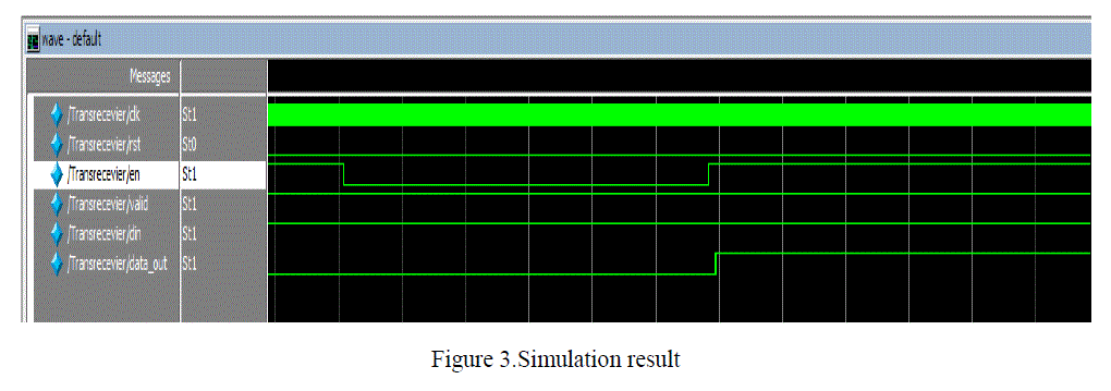
| Figure 3 shows the FPGA output of the implemented design. The figure 3 shows the simulated waveform of
transceiver, input is given as 1 serial input and we get the same value at the transmitter output when enable is high. |
 |
CONCLUSION |
| In this paper we present the design of a transmitter, receiver and 3.2Gbps Viterbi Decoder suitable for IEEE 802.15.3c
transceivers. Results show that Xilinx FFT Pipelined/Streaming I/O architectures, combined with Radix-2 operations,
and the sliding-block method with two parallel VD for each of the eight decoding channels permits to meet IEEE
802.15.3c requirements for a receiver. All designs were implemented on SPARTAN 3 FPGA. All the architectures will
be used on the current development of an IEEE 802.15.3c receiver. |
References |
- H. Singh, Jisung Oh, ChangyeulKweon, Xiangping Qin, Huai-Rong Shao and Chiu Ngo, "A 60 GHz wireless network for enabling uncompressed video communication", IEEE Communications Magazine, vol. 46, Issue 12, pp. 71 - 78, 2008.
- Ruben Cabral, "Matlab/Simulink wireless HDMI model and simulation", MsC thesis, Instituto Superior T̮̩cnico, October 2011.
- Part 15.3: Wireless Medium Access Control (MAC and Physical Layer PHY) Specificications for High Rate Wireless Personal Area Networks WPANs", October 2009, [Online]. Available:http://standards.ieee.org/getieee802/download/802.15.3c-2009.pdf.
- Bruno Fernandes and Helena Sarmento, âÃâ¬ÃÅFPGA implementation and testing of a 128 FFT for a MB-OFDM receiverâÃâ¬ÃÂ, Analog Integrated Circuits and Signal Processing, Vol. 70, NÃâú 2, 241-248, September 2011.
- Tzu, K.-H. and Dunham.J. âÃâ¬ÃÂSliding Block Decoding of Convolutional CodesâÃâ¬ÃÂ, in IEEE Transactions Communication, vol.COM-29, pp. 1401-1403, Sep.-1981.
- Bo Gao; Zhenyu Xiao; Changming Zhang; Li Su; Depeng Jin; Lieguang Zeng, âÃâ¬ÃÅPerformance comparison of channel coding for 60GHz SC-PHY and a multigigabit Viterbi decoderâÃâ¬ÃÂ, International Conference on Computational Problem Solving., 2011, pp. 714-718.
|