International Journal of Innovative Research in Science, Engineering and Technology
ISSN ONLINE(2319-8753)PRINT(2347-6710)
ISSN ONLINE(2319-8753)PRINT(2347-6710)
B.T.Jayalakshmi1, S.Vamsee Krishna2
|
| Related article at Pubmed, Scholar Google |
Visit for more related articles at International Journal of Innovative Research in Science, Engineering and Technology
Analog-to-digital converters have many applications in our daily life. The Sigma-Delta converter is an attractive ADC for future communication systems due to its high number of bit rate. The aim of this project is to design of sigma-delta ADC and it is implemented using SPARTAN 3e FPGA.In this project sigma-delta conversion can be done by using the advanced IC MCP3208 and bit by bit transmission is done finally the output is displayed on monitor of pc.The main aim of this project is to power reduction and the converter is used to achieve 12-bit resolution. In MATLAB Simulink the converter done but greater filter delay in the output and it is not suitable for FPGA implementation. To overcome this problems sigma-delta conversion is done using the Xilinx ISE design tool 14.6 and the power comparison calculation is done. In its supply voltage 5v, analog input is taken as potentiometer, by varying the input voltage(12-bits)0-2^12 that means up to 4096 range, through rs232 cable, the output is displayed on monitor. The sigma-delta analog-to-digital converter is suitable for embedded FPGA applications. The sigma-delta architecture has become more and more popular realizing high-resolution ADCs in mixed-signal VLSI processes. This converter is inherently an oversampling converter, although sigma-delta converter is just one of the techniques contributing to the overall performance
Keywords |
| Analog-to-digital converter (ADC),Field programmable gate arrays (FPGA), Sigma-Delta, VLSI, User Constraint File (UCF). |
INTRODUCTION |
| Analog-to-digital converters play an important role in modern audio and communication design. Nyquist converters are used efficiently only for medium resolutions and require analog components that are precise and highly immune to noise and interference. On the other hand oversampling converters are achieve high resolutions(>20bits).In conventional modulators, negative feedback is applied, to control the dynamic behaviour of a system and to realize the attenuation of the quantization noise in the signal band due to noise shaping. With the increasing demand of electronics product, thecircuits are complexity to growing high. The competitive pressures available time to design products is shrinking. Field programmable gate arrays (FPGA) provides best solution to address all these issues. Field programmable gate arrays are able to offer advantages over traditional VLSI technology. |
RELATED WORK |
| Analog-to-digital converters are classified in two classes: (1) Nyquist rate ADC (2) Oversampled (Sigma Delta) ADC. There are some drawbacks in Nyquist rate converters as follows: |
| Medium Resolution |
| Require Analog components |
| High noise |
| High Interference |
| In Nyquist-rate ADC the input analog signal samples at the sampling frequency (fs) is equal to the twice of the highest frequency component of the input signal. It is necessary for the input signal to band limited; an anti-aliasing filter must be used before the converter to prevent aliasing. This filter must have a very narrow transition band to ensure that the filtered signal does not contain any frequency component above fs/2.But to realize narrow transition band anti-aliasing filter is very difficult. Also Nyquist rate converters have low resolution which is not suitable for a very low voltage signal conversion. Oversampled ADCs are preferred over Nyquist rate ADC due to their high signal to noise ratio and high resolution [4]. |
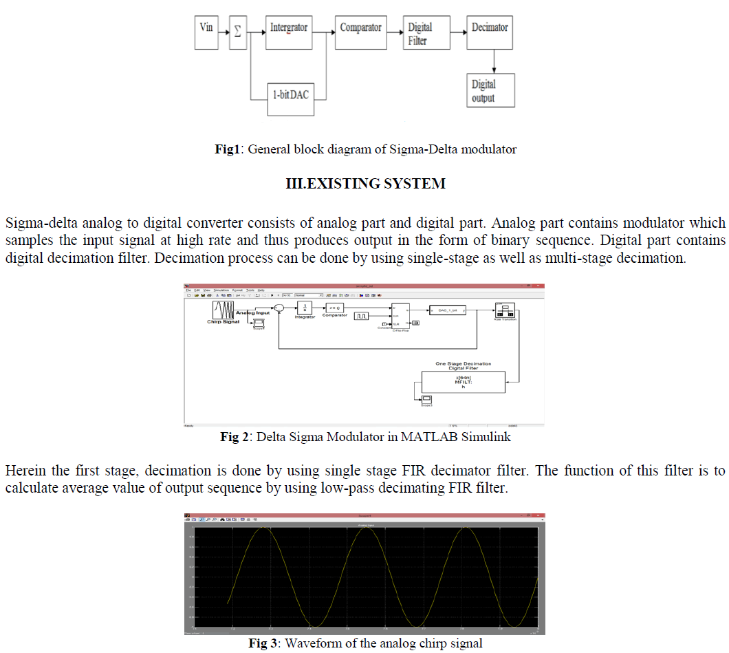
| In case of sigma-delta ADC the modulator portion behaves like a noise shaper and digital filter removes the out of band quantization noise thus ensure much higher SNR which is impossible to achieved in Nyquist ADC[5].In addition to improve SNR,sigma-delta ADC inherently possesses the motivation for prediction. When the signal is oversampled then it does not change significantly in the interval between successive samples [6].Since the values of these samples are very close, they are highly correlated and there are future samples could be predicted from the past one. The linear delta modulator is the simplest predictive modulator. By pushing most of the in-band noise outside the signal frequency band more improvement in the SNR can be achieved. This is attainable if signal transfer function is a low pass whereas and Noise transfer function is high pass. This method is called noise shaping and can be easily and efficiently implemented by modifying the delta modulator[7].Here integral of the input signal encoded rather than input signal directly. Clearly integration is a linear function does not affect system transfer function. The demodulation integrator at output can be placed at the input of delta modulator. This modification of delta modulation system results to the new system called Sigma Delta Modulator as shown in figure1. |
 |
 |
 |
 |
 |
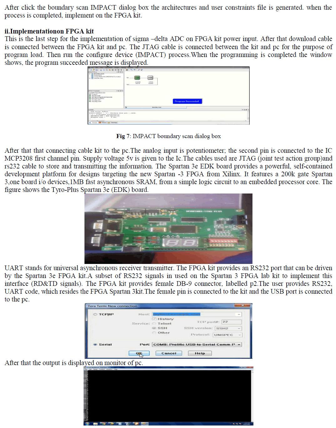 |
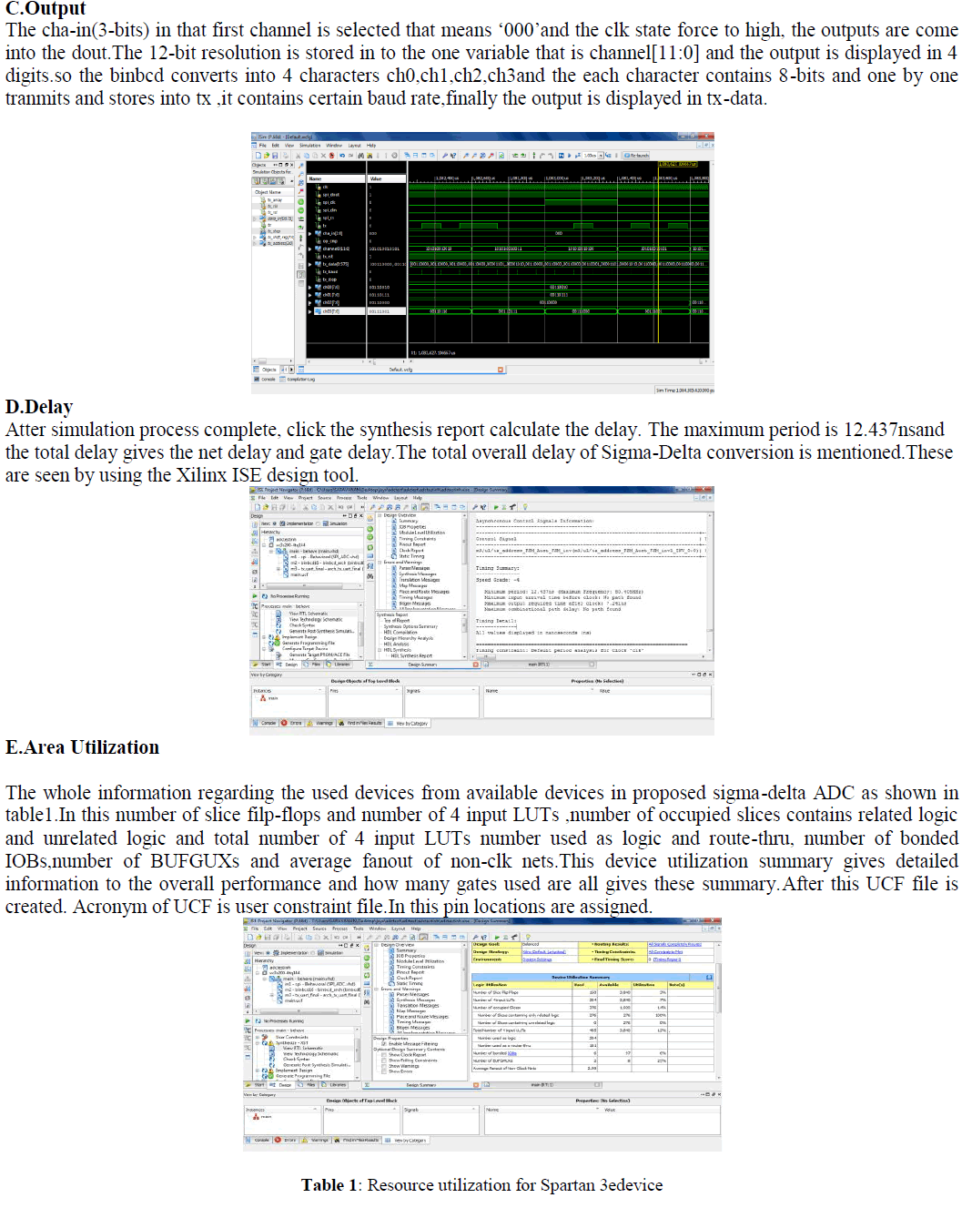
| The output is displayed on monitor by using the tera term software. Here using two cables one is rs232 and another one is JTAG cable. For program load purpose the JTAG is used. The parallel port is connected to the pc and the JTAG is connected to the FPGA kit. Finally the output is displayed on monitor of pc.The output is displayed between the range 0-4096 range only(12-bits)resoultion. |
CONCLUSION |
| In this, we have designed of Sigma-Delta ADC and its implementation on SPARTAN 3eFPGA kit. It consumes only 150 number of slice Flip Flops out of available 3,840, 304 number of 4 input LUTs out of 3840 and 276 number of occupied slices out of 1,920 and number of slices containing only related logic 276,number of slices containing unrelated logic is 0 and total number of 4 input LUTs are 485 out of 3,840 in that number used as logic is 304 and number used as route-thru 181.Number of bonded IOBs 6out of 97 and number of BUFGMUXs is 2 out of 8 and average fan out of non-clock nets 299 respectively. The proposed design power consumption is 350uw.Results shows that the proposed design is quite accurate. |
References |
|