Keywords
|
| Circuit parameters,Finite elements, Frequency sensitivity,Planar device, Substrate Integrated Waveguide (SIW). |
INTRODUCTION
|
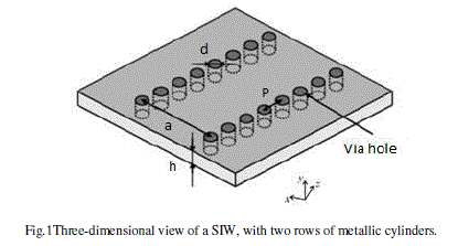
| The Substrate-Integrated Waveguide(SIW), also called post-wall waveguide or laminated waveguide, is a promising candidate for millimetre-wave and terahertz application. This periodic waveguide, as illustrated in Fig. 1, is composed of two rows of conducting cylinders embedded in a dielectric substrate that connect two parallel metal plates. The first mention of this type of waveguide, to the best of the authors’ knowledge, dates back to 1994 [1]. Since that time, a vast range of SIW components, such as filters, antennas, transitions, couplers, power dividers, and oscillators, have been proposed and studied. Such SIW structures can largely preserve the well-known advantages of conventional rectangular waveguides, namely, high-Q factor and high power capacity. |
 |
| In this paper we describe how Foster reaction theorem and finite element can be used to calculate sensitivity of a SIW to frequency using data of a single simulation only and at a little extra computational cost. |
| A planar device can be defined as one in which electromagnetic fields do not vary significantly in one dimension [2- 3] so that the simulation can be carried out in a plane. Substrate-integrated waveguide at dominant mode is an example of a perfect planar device. |
| Determining frequency sensitivity can be helpful in broadband calculation of circuit parameters.Since, in each simulation beside the circuit parameters their sensitivity relative to frequency is calculated. In resonant structures calculating frequency sensitivity due to change in structure parameter can be very useful for tuning bandwidth. Further, there have been some attempts at getting a computer to predict the best shape for a planar device, i.e., predicting the shape that minimizes return loss, gives a specified phase shift or division of power, and so on, where frequency sensitivity can be help to calculation the best shape for a planar device. |
ANALYSIS OF SIW
|
| The basic structure of the substrate integrated waveguide is the laminate with a waveguiding channel having an array of metallic vias. SIWs maintain the advantage of metallic waveguides like low losses and high power capacity, in addition combining them with the possibility of integration typical of microstrip structures. |
| A. Design Techniqueof SIW |
| Substrate integrated waveguide is made of a periodic via structure to realize bilateral edge walls. This periodic structure is much more complex for analysis than the conventional waveguide. Simulations of the integrated waveguide using a finite element method require abundant resources and the design of such a waveguiding structure is not straightforward. To improve the design efficiency, we transform the SIW to an equivalent rectangular waveguide. |
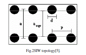 |
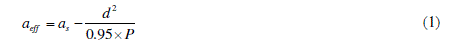
| Theequivalent width of the SIW isprovided by following equation withvery good approximation [6].Where,P is sufficiently small. |
 |
| B. Components Design |
| Substrate integrated waveguidecomponents presented in this part are all designed on a Rogers RT/duroid 5880, with εr=2.2 and Thickness 0.787 mm. According to figure 2, the via diameter is d = 0.3mm and the pitch is p = 0.6mm. The distance of the bilateral via sidewalls is a = 6.686 mm. With the selected dimensions, we obtain an equivalent waveguide of dimension equal to aeqv=6.528mm. |
| C. Frequency Sensitivity of a SIW |
| Because the final objective is to calculate the frequency sensitivity of SIW, we first begin by defining voltage and current at the SIW ports. We assume ei and hi are tangential electric and magnetic field at port idue just to the dominant mode wave incident on port i, when this wave carries unit real power into the junction region. |
| Generally, tangential electric and magnetic field on port iare: |
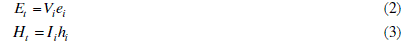 |
| This provides our definition of voltage Viand current Ii at port i. It can be shown that the admittances and impedances we compute are normalized to wave impedance of the guide [3]. In view of thestructureshown in Fig.1and according tothe SIW at dominant mode is a perfectly planar device. In this paper, assumed field do not vary significantly in y dimension so the electric field can be represented as: |
 |
| where,ay is a unit vector in y dimension. Substituting (4) into the time-harmonic Maxwell'sequations, find that the equation governing E is: |
 |
| It is simplifiedto 2-D scalar wave equation as below: |
 |
| where,Ω is area of the device, ∂ΩD1 is Dirichlet excitation interface, ∂ΩD2 is electric wall, ∂ΩNis magnetic wall and E0 equals prescribed value of electric field due to unit power. It has been shown that solving the Eq. (6) is equivalent to solving the following variation problem [5] |
 |
| Alternatively, it has been shown in [7] that the solution to the above equation is the stationary point of a functional: |
 |
| This is the basis of the finite element analysis of SIW. By introducing functional, (8)is reduced to a matrix form: |
 |
| where,[S] and [T] are well-known finite element global matrices [7-8]. After applying boundary condition it reduces to the form of [A].[E]=[b]. Solving the equation yields electric field on device. In addition,In [9] has been shown by the means of foster theory of reaction that susceptance sensitivity of a lossless device with respect to angular frequency can be calculated as: |
 |
| where,We and Wm are average electric and magnetic energy respectively.If substitute the planar electric field from (1-3) it reduces to: |
 |
| where m, n are port numbers, b is dimension of structure in y direction, Ãâ Þ0 is intrinsic impedance of free space, [Smn] is normalized sensitivity matrix and E(k)is electric field when there is normalized voltage on port k.Using triangular elements it reduces to the following equation: |
 |
| where[S] and [T] are well-known global matrices [7-8]. By means of (12) using the same data from simulation sensitivity of network parameters is calculated in addition to network parameters themselves. |
RESULTS
|
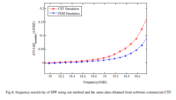
| A computer program has been written to implement above numerical method, single examples has been selected to verify the method in each case numerical results are compared with results of commercial software. |
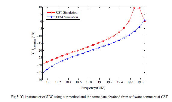 |
 |
CONCLUSION
|
| It has been shown simulation data not only can be used for circuit parameters extraction, but also can be used in achieving frequency sensitivity. Frequency sensitivity can be lead to structure shape optimization. Determining frequency sensitivity can be helpful in broadband calculation of circuit parameters. Since, in each simulation beside the circuit parameters their sensitivity relative to frequency is calculated.In this paper, the equivalent circuit parameters of the SIW line has been calculated utilizing triangular FEM. Moreover, the frequency sensitivity of the equivalent circuit parameters has been also determined. Good agreement has been obtained with results of commercial software. |
ACKNOWLEDGMENT
|
| The authors would like to thank BehroozZaker and ErfanMaaliAmirifor the advice and support they have given during the work. |
References
|
- D. Deslandes, and K. Wu, "Accurate Modeling, Wave Mechanisms, and Design Considerations of a Substrate Integrated Waveguide," IEEE Transactions onmicrowavetheoryandtechniques, vol. 54, no. 6, pp. 2516-2526, June 2006.
- P. Garcia and J. P. Webb, “Optimization of Planar Devices by the Finite Element Method,” IEEE Transactions on Microwave Theory and Techniques , VOL. 38, NO. 1, Jan 1990.
- J.P. Webb and S. Parihar, “Finite element analysis of H-plane rectangular waveguide problems,” Proc. Inst. Elec. Eng., vol.133, pt. H, pp. 103-109,Jan. 1986.
- F. Xu and K. Wu, "Guided-Wave and Leakage Characteristics of Substrate Integrated Waveguide," IEEE transactions on microwave theory and techniques, vol. 53, no. 1, pp. 66-73, January 2005.
- D.Deslandes and K. Wu,"Design Consideration and Performance Analysis of Substrate Integrated Waveguide Components, "Proc. Inst. Elec. Eng., vol.133, pt. H, pp. 103-109,Jan. 2006.
- Y. Cassivi, L. Perregrini, P. Arcioni, M. Bressan, K. Wu, and G. Conciauro, "Dispersion characteristics of substrate integrated rectangular waveguide," IEEE Microw. Wireless Compon.Lett, vol. 12, no. 9, pp. 333–335, Sep 2002.
- J.M. Jin, "The finite element method in electromagnetics", Wiley, 2002.
- Matthew N. O. Sadiku, "Numerical techniques in electromagnetics", CRC Press, 2000.
- R. E. Collin, Foundations for Microwuve Engineering. New York: McGraw-Hill, 1966, p. 147.
- M.Bozzi, L.Perregrini, K.Wu, "Modeling of conductor,dielectric and radiation losses in substrate integrated waveguide by the boundary integral-resonant mode expansion method," IEEE Trans. on Microwave Theory and Techniques, vol. 56, no. 12, pp. 3153-3161, 2008.
- K.Wu and D. Deslandes, "The Substrate Integrated Circuits - A New Concept for High-Frequency Electronics and Optoelectronics," IEEE TELSIKS International Conference on, vol. 54, no. 6, pp. 2516-2526, Dec 2003.
|