The main source of power in a Satellite is the Solar Array. Spacecraft which uses Photovoltaic cells is usually equipped with Rechargeable batteries that receive a charge from Main bus when Solar panels are in sunlit condition. During eclipse, the Shunt regulator remains off and Battery serves the Spacecraft load, which lowers the battery voltage. All these create a varying DC as the Spacecraft Bus Voltage. A Battery Charge and Discharge Control are required to maintain battery voltage within acceptable limits and extract maximum life out of the Battery. Typically, separate hardware circuits are used for the Battery Charge Regulator (BCR) and Battery Discharge Regulator (BDR). This paper discusses a Battery management scheme using a BCR/BDR Bidirectional converter.
Keywords |
| Bidirectional control, Battery management system, regulators, Battery Charge Regulator, Battery
Discharge Regulator. |
INTRODUCTION |
| The primary source of power for any spacecraft is solar array, because it is abundantly available in space and its
conversion process easy compared to other potential options for primary sources. Solar array system is usually
combined with rechargeable batteries as secondary source to serve the load during eclipse. This system is also known
as Photovoltaic-battery system. Photovoltaic cells work on the principle of photoelectric effect i.e., generation of
electricity due to the absorption of light (photons) by the semiconductor material used in the PV cells. The DC voltage
generated by the solar array is dependent on availability of the sun‟s radiant energy; the energy received by the PV cells
varies with square of the distance from Sun. PV cells are arranged in series–parallel combinations to obtain the desired
voltage and current. In the presence of solar radiation, the solar array source the power bus, which is sources loads
connected to it and at the same time charges the battery. When eclipse occurs, PV cells come under shadow, which is
equivalent to the absence of the input source. In this condition, the battery which was charged earlier will start sourcing
the power bus. |
RELATED WORK |
| In the presence of sunlight, the input voltage is a variable because of the variation in the illumination level. A regulated
voltage is provided for the charging of the battery, this is done by Battery charge regulator [1]. Since VBUS >VBAT, it has
to be stepped down to match the battery voltage. The output voltage obtained should always be less than the applied
input and the DC-DC converter used for this purpose is Buck converter. So, the battery charge Regulator performs the
function of step down converter. During the eclipse, solar array input will be unavailable. The battery serves the bus,
Since VBAT < VBUS; VBAT has to be stepped up or boosted to bus voltage level. This is accomplished by Battery
discharge regulator [1]. |
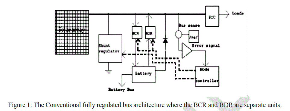 |
| Figure 1, shows the conventional fully regulated bus architecture where the battery charge regulator and discharge
regulators are separate units. By combining it in a single topology, the space and cost of the module is reduced. In
paper [3] Six different topologies of bidirectional converter using two switches and two inductors are explained, where
one out of six configurations can be used as Bidirectional BCR/BDR. This paper has considered two conditions, VBAT
>VBUS and VBAT < VBUS. |
PROPOSED TOPOLOGY |
| To achieve the Battery charge and discharge regulator operations in a single topology, a Bidirectional DC-DC
converter is in series with solar array and battery as shown in figure 2. At the input side, strings of solar array are
connected in parallel with shunt switches across each string. Bus voltage has to be maintained at a constant voltage of
28V. |
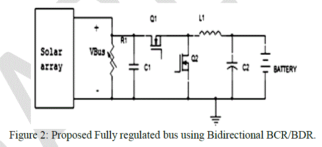 |
| Figure 2 shows the proposed fully regulated bus using Bidirectional BCR/BDR circuit. It is assumed that the
VBUS>VBAT for this circuit. The power bus will be connected to various loads and battery is one of the loads. But this
paper is focusing on the battery part only. There is no fixed input side and output side, during BDR mode the battery is
input and power Bus is the output. During BCR mode, solar array in the input and power bus, battery are the output.
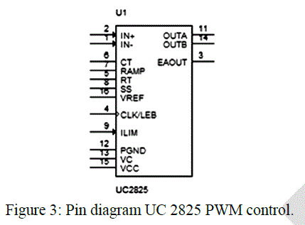
The circuit consists of two switches and one inductor. The switching of the converter operations are controlled by
PWM Controller IC. UC 2825 PWM IC shown in figure 3 is employed for the control of the switching converters. UC
2825 is a high frequency PWM controller; the operating frequency can be set up to 1MHz and it is compatible with the
voltage mode or current control mode techniques. In voltage control mode, the dc output voltage is the feedback signal
and it will be compared with the predetermined dc voltage reference and the difference of these two signals gives rise
to amplified error signal. A control signal is generated and it controls the pulse width of the gate pulses. Therefore, the
conduction time of the switches is controlled by varying the duty cycle. The closed loop operation takes care of the
conduction time of the switches in both the modes. The operating frequency is programmed to desired value by
connecting appropriate values of timing capacitor CT and timing resistor RT [2]. This IC has two regulated output ports
OUT A and OUT B. the special feature of the IC are the integrated error amplifier, soft start current mode control. The
duty cycle that can obtain at each output pins is max of 50%. The pin diagram of the IC is as shown in figure 3: |
 |
| The PWM pulses obtained at OUT A is used to drive the switches. The switches are selected such that it is capable
allowing the current to flow in both the directions. N-channel MOSFETs are used as power switches. The PWM output
is connected to the primary of the transformer and the secondary is connected as gate to drive the switch. The drive for
the shunt switch is obtained by complementing the OUT A. |
| A. Battery Discharge regulator Model |
| Initially it is considered that the solar array input is absent, because the solar panels are yet be deployed. Battery serves
the load until the solar array input is available. In BDR mode of operation, the battery voltage VBAT is boosted to VBUS
level. Series switch Q1 is open and Shunt switch Q2 is closed in this mode. |
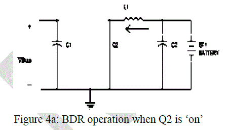 |
| The Battery is the input source and bus is load. C2 is the input capacitor and C1 is output capacitor. Inductor is
common for both BCR and BDR. L1 is the input inductor. Figure 4a shows the operation of the BDR when the switch
Q2 is „on‟, the battery current IBAT flows through the inductor L1 and it stores energy in the form of magnetic field. The
inductor voltage will be equal to the input voltage. |
 |
| Figure 4b shows the BDR operation when the switch Q2 is „off‟ the energy stored in the inductor and the input energy
together form the output voltage. The load is sourced by both input source as well as energy stored in inductor L1. The
energy from the inductor and input is carried to the load through the diode, because diode will be forward biased in this
duration |
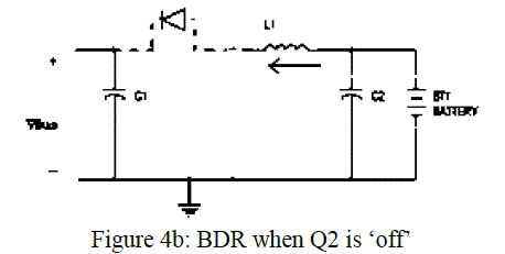 |
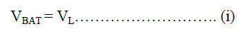
| VBUS = VL+VBAT……………………. (ii) |
| The battery voltage ranges from 18-24V and it is boosted to 28V. VBUS is given as the feedback signal and it made sure
that is regulated, this by done by choosing appropriate ratio of resistors at the voltage divider. |
| B. Battery Charge Regulator Model |
| During sunlit condition, the solar array provides the necessary power required by the load and also it charges the
battery. Since VBUS>VBAT, the bus voltage is reduced by some value to match up to the battery requirement. This is
done by battery charge regulator (BCR). During the BCR mode, the series is conducts and shunt switch remains open. |
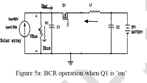 |
| Figure 5a shows the BCR operation when switch Q1 is „on‟, the input current flows through L1 and to the battery. L1
stores energy in TON duration. |
| VL= VIN-VBAT………… (iii) |
| VL= -VBAT………….. (iv) |
| Figure 5b shows BCR operation when Q1 is „off‟, input is absent and energy stored in the inductor freewheels through
the circuit and sources the load. Inductor voltage during on period is given by equation (iii) and Inductor voltage during
off period is given by equation (iv). The negative sign in the equation (iv) indicates the direction of current flow. |
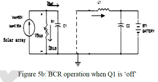 |
| There are two loads to be served by the solar array, the power bus and the battery. The input current is shared by the
bus IBUS and battery IBAT. If the solar array alone cannot serve the load requirement, battery starts supporting the load
along with solar array input. At this condition, battery is in discharging mode even in the presence of sunlight. |
EXPERIMENTAL RESULTS |
| Specifications: VBUS = 28V, VBAT=18-24V, f=100 KHz, L1= 78μH, C1=168μF & C2= 86μF, Q1, Q2= N-channel
MOSFET. |
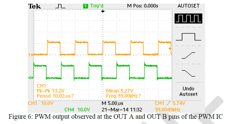
| The PWM output is obtained at the pin 11 (OUT A) and pin 14 (OUT B) of the IC. To obtain the PWM pulses, the
desired frequency is programmed by connecting timing resistor RT =3.9KΩ and timing capacitor CT= 2.2F. The
maximum duty cycle of each output can be up to 50%, the duty cycle of the waveforms shown in Figure 6 is about 45%
and magnitude is 12V and operating frequency is 100 KHz. There is 180 degree phase shift between the output
waveforms. Figure 6 shows the PWM output at both output pins. |
 |
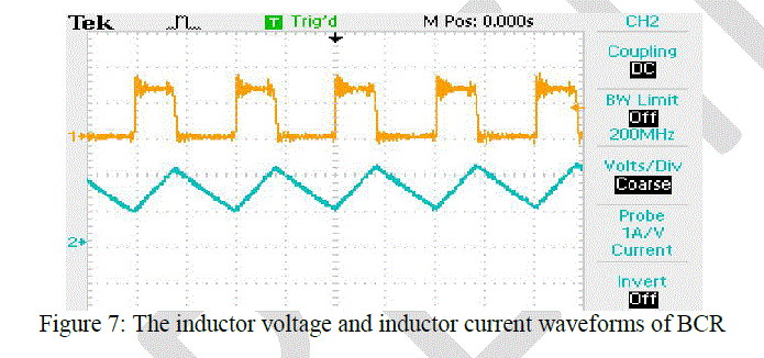 |
| Figure 7 shows the Inductor voltage VL and inductor current IL waveforms. When the switch Q1 is „on‟, the current
starts flowing through the inductor and inductor voltage VL is observed during TON duration and during TOFF duration
diode voltage drop of about 0.4V appears across the inductor, which is negligible and almost equal to zero. The
inductor current waveform is the sum of output current with current ripple. The ripple is due to charging and
discharging action of the energy stored in the inductor. |
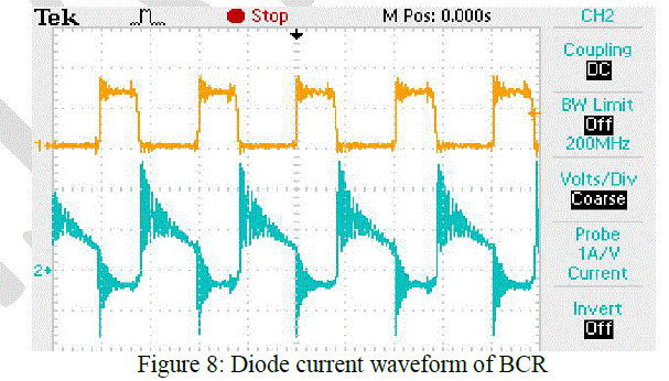 |
| In figure 8, the inductor voltage waveform is taken as reference to show that the diode conducts during TOFF time.
During TON duration, Q1 conducts and diode is in reverse biased condition. So during TON condition, diode does not
conduct and it is observed from the above waveform that the diode conducts only during TOFF duration. |
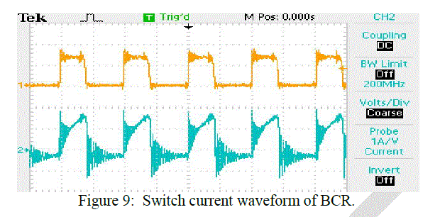 |
| Figure 9 shows the switch current waveform. The switch conducts during TON duration and it is open during TOFF.
The inductor voltage VL is kept as reference to compare the „on‟ and „off‟ time durations. |
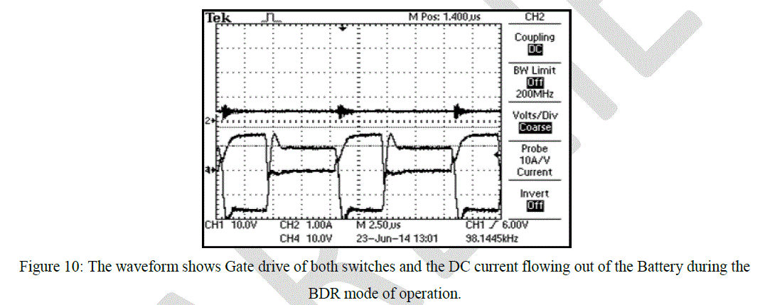 |
| Figure 10 shows the waveforms of Gate drives of series and shunt switches. The duty cycle of the series switch which
drives Q1is about 75% and duty cycle of the shunt switch which drives Q2 is about 23%. The duty cycle need not be a
constant or fixed; it may vary to make sure that a regulated voltage is obtained at the output. The DC level is the current
flowing out of the battery is positive during the Eclipse, indicating that the battery is in discharging mode. |
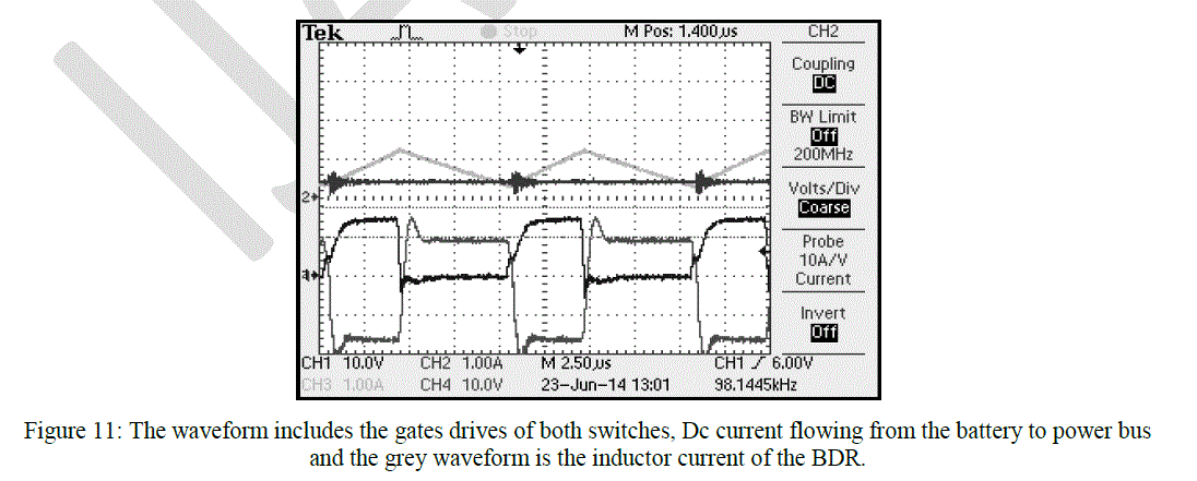 |
| Figure 11 shows the Gate drives, current flowing out of the battery and the inductor current of the Battery discharge
regulator. From the figure it is evident that the inductor current is gradually increasing when the shunt switch is „on‟
and current decreases when the switch is „off‟. |
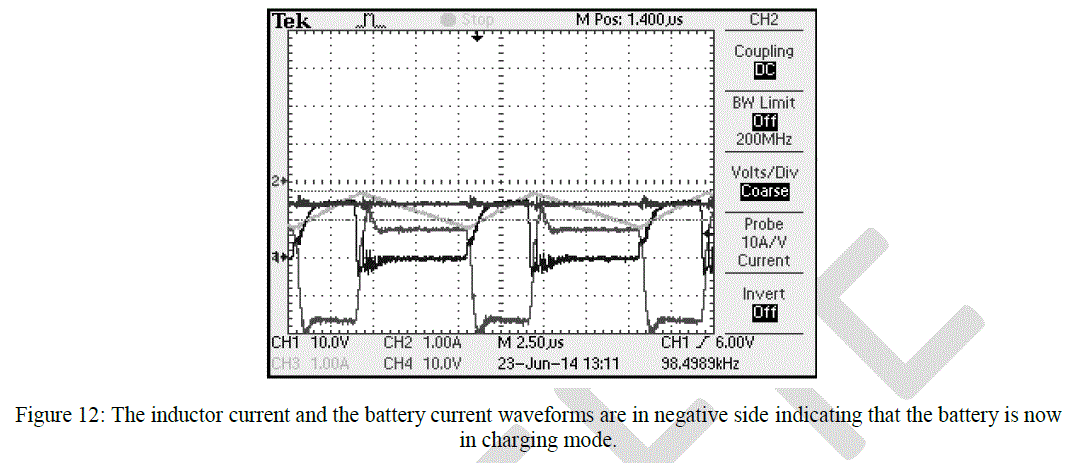 |
| Figure 12 shows the change in the polarity of the inductor current IL and battery current IBAT. When the Solar array
input is available, the current contribution from the battery reduces and as the solar array input increases, it is capable
of serving the power bus as well as charging the battery. The negative polarity of the battery current IBAT indicates that
the battery has now entered charging mode. Inductor current polarity shows that the mode of operation has changed;
Battery discharge regulator will now perform the function of Battery charge regulator |
CONCLUSION & FUTURE SCOPE |
| Previously, separate battery charge and discharge regulators were used for charge/discharge management. The
advantage of combined operation of BCR/BDR in the same converter topology alone will be realized in this paper.
Since it works in closed loop, this system is more efficient and reliable. The voltage applied as input to the regulator is
generally variable but higher than the spacecraft‟s required constant bus voltage. The regulator converts excess
electrical energy into heat which is radiated away into space. The advantage of combined operation of BCR/BDR in the
same converter topology is realized in this paper. The developed module thus needs fewer components, less space, less
cost of fabrication and lesser testing time. Thereby totally reduces the launch cost of spacecraft. A single PWM
controller is implemented to control both the BDR and BCR operation. Power Buses of higher power ratings can be
designed and implemented. |
ACKNOWLEDGEMENT |
| On my way towards the accomplishment of this project work, I want to express my gratitude to people who have
been involved directly or indirectly in this project and made this project possible. |
| I wish to express my deep sense of gratitude to my guide, Dr. Usha P, Professor, Department of Electrical and
Electronics, D.S.C.E, Bangalore who has been a source of inspiration throughout two years of degree and given her
valuable guidance and suggestions. |
| I would also like to extend my special thanks to all the teaching and non-teaching staff of Dayananda Sagar
College Of Engineering (D.S.C.E), Bangalore. |
| I would like to express my heartfelt thanks to my beloved Parents for supporting me emotionally and morally
during the course of this project. |
References |
- Mukund. R. Patel: âÃâ¬ÃÅSpacecraft power systemsâÃâ¬ÃÂ, CRC press, USA 2005.
- UC 2825 Datasheet
- J. Calvente, L. Martinez-Salamero, P. Garces, R. Leyva and A. Cape1Department &Enginyeria Electronica, ElectricaiAutornatica, ALCATEL SPACE INDUSTRIES :âÃâ¬Ã Dynamic Optimization of Bidirectional Topologies for Battery Charge/Discharge in SatellitesâÃâ¬ÃÂ, 0-7803-7067-8/01/$10.00 02001 IEEE, Page 1994-1999.
- www.ti.com
- www.irf.com
- www.mag-inc.com
- www.en.wikipedia.org
- S.H.Weinberg1, A.Lopez2,2CRISA S.A- Madrid-Spain,âÃâ¬Ã A Bidirectional BDR/BCR for satellite applicationsâÃâ¬ÃÂ, Proceedings of the Fifth European Space Power Conference,Tarragona,Spain,21-25September 1998,ESA SP-416,September 1998,Page 27-32.
- N. Mohan,T. UndelandRiobbins, Power Electronic- converters, Applications and Design, - Wiley âÃâ¬ÃâIndia edition.
- David A Bell, Operational Amplifiers and Linear ICs, second edition.
|