International Journal of Advanced Research in Electrical, Electronics and Instrumentation Engineering
ISSN ONLINE(2278-8875) PRINT (2320-3765)
ISSN ONLINE(2278-8875) PRINT (2320-3765)
E.Kanniga1, N. Imocha Singh2 and K.Selva Rama Rathnam3
|
| Related article at Pubmed, Scholar Google |
Visit for more related articles at International Journal of Advanced Research in Electrical, Electronics and Instrumentation Engineering
With the progress of VLSI technology, delay buffer plays an important role affecting the circuit design and performance. This paper presents the design of low power buffer using clock gating and gated driver tree. Since delay buffers are accessed sequentially, it adopts a gated clock ring counter addressing scheme. The ring counter employs double edge triggered (DET) flip flops instead of traditional flip flop to half the operating frequency. Also for generating clock gating signals, combinational elements (C-element) are implemented in the control logic to avoid the increasing loading of the global clock signal. For the clock distribution network, a gated driver tree technique is used and it further reduces the power consumption. In addition, this technique is used in the input and output ports of the memory to decrease their loading. The proposed delay buffer consumes less power comparing to the conventional delay buffers.
INDEX TERMS |
| C-element, DET flip flop, delay buffer, clock gating, gated driver, ring counter. |
INTRODUCTION |
| Due to the massive usage of portable battery operated, design of low power circuits has become an important one factor in modern VLSI technology. For these products, delay buffers which are also line buffers and delay lines are used. In the temporary storage of signals that are processed such serial access memory is needed. |
| To compensate for the difference in the rate of being flow of date, holding data for use at a later timing, allowing timing corrections to be made on data stream, delaying the transit time of signal in order to allow other applications to occur delay buffers are used. Currently, most circuits adopt static random access memory (SRAM) plus some control/addressing logic to implement delay buffers. For smaller-length delay buffers, shift register can be used instead. In the long delay buffers SRAM-based delay buffers are more popular because of the compact SRAM cell size and small total area. There still can be considerable power consumption in the SRAM address decoder and the read/write circuits. |
| In the proposed delay buffer, a gated clock ring counter is used to access the memory. Instead of single edge triggered flip flop, the ring counter uses double edge triggered (DET) flip flop to half the operating clock frequency. In the control logic for generating the clock gating signals to avoid the increasing loading of the global clock signal, combinational element (C-element) is used. In addition to gating the clock signal going to the DET flip flops in the ring counter, a gated clock driver tree is then applied to further reduce the activity along the clock distribution network. If no gating is applied, all drivers need to be activated. A driver tree distribution network is used for the global clock and activate only those drivers along the path from the clock source to the block that need to be activated by the clock[5]. This technique will greatly decrease the loading on distribution network of the clock signal for the ring counter and thus the overall power consumption. The same technique is applied to the input driver and output driver of the memory part in the delay buffer. For the input circuitry, in each level of the driver tree, only one driver along the path leading to the addressed memory word is activated. |
| Similarly, only one driver along the path from the addressed memory word to the output is activated for the read circuitry in each level of driver tree. Thus, the power wasted on the drivers can be eliminated that need not to be activated by this technique. |
CONVENTIONAL DELAY |
| BUFFERS |
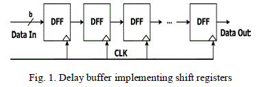
| For implementing short delay buffers where area and power are of less importance, shift registers are used. Upon the application of clock pulses, data in the shift register can be moved.[2] |
 |
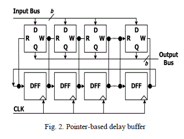
| In the pointer based design, a ring counter with only one rotating active cell to point the words for write-in and read-out. The bottom row of DFF is initialized with only one “1” and all the other DFFs are kept at “0”. When a clock edge triggers the DFFs, this “1” signal is propagated forward. Consequently, the traditional binary address decoder can be replaced by this “unary-coded” ring counter. Compared to the shift register delay buffers, this approach propagates only one “1” in the ring counter instead of propagating - bit words.[2] |
 |
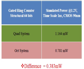
| In the Oct system, i.e. every 8 DFFs in the ring counter are grouped into one block for the gated clock technique. Then, a gated signal is computed for each block to gate the frequently toggled clock signal when the block can be inactive so that unnecessary power wasted is eliminated.[2] |
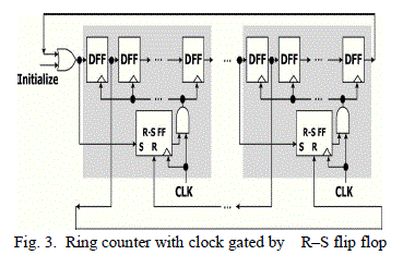 |
| As shown in fig. 3, when the input of the first DFF In the block is set to “1”, it sets the output of R–S flip flop to “1” at the next clock edge. Thus, the incoming “1” can be trapped in that block and continue to propagate inside the block. Contrary to this, when this block is active, other blocks are shut down. The successful propagation of “1” to the DFF in the next block can shut down the unnecessary clock signal in the current block. This technique of gated clock ring counter and gated driver are used to reduce power consumption during data write in or read out. |
GATED CLOCK RING COUNTER |
| The ring counter which uses DET flip flop and C-elements are used for the generation of clock gating. To further reduce the activity along the clock distribution network, a gated clock driver tree is then applied. [2] |
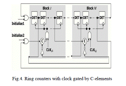 |
| In the fig.3, extra R-S flip flop still consume more power. So, it is replaced by C-element as in fig.4. Saving more power. |
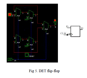
DET flip flop |
| Double edge triggered flip flops are used instead of a Single edge triggered flip flop in the ring counter. Double edge triggered flip-fops are used to generate two outputs at a single clock pulse. In these flip-flops work will be done at rising edge and falling edge. Thus, clock frequency is reduced to one half. |
 |
CLOCK GATING USING C-element |
| A gating function is used to turn off the clock to some of the functional module for some extended period of time. |
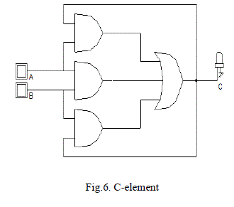 |
| The logic express for C-element [5] is given by |
| Cnext = AB + BC + CA |
| where A and B are its inputs and C and Cnext is the current and next output. If A=b, then the next output will be the same as the input. Otherwise, if A≠B, then output remains unchanged. Since the output of C-element can only be changed when A=B, it can avoid the possibility of glitches. It’s avoiding excessive clock loading. It’s works with hand shaking protocol. |
GATED CLOCK DRIVER TREE |
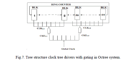 |
| Loading on the global clock signal “CLK” is diminished further by using this technique. This method efficiently reduces the length of clock path that distributed in whole circuit and distribution layers also get reduced by which the tree contains 8 leaf. A driver tree distribution network is used for the global clock and activated only those drivers along the path from the clock source to the blocks that need to be driven by the clock. |
GATED DRIVER TREE FOR INPUT AND OUTPUT |
| This technique can eliminate the power wasted on the drivers that need not be activated. Of all the memory cells, only two words will be activated: one is written by the input data and the other is read to the output. |
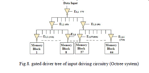 |
| Driving the input signal all the way to all memory cells seems to be a waste of power. The same is in the case of read circuitry of the output port. In the input driving/output driving sensing circuitry in the memory module of the delay buffer, the gated clock tree technique is used. |
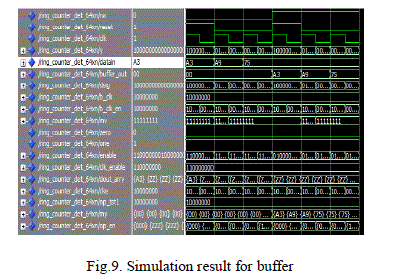
RESULTS |
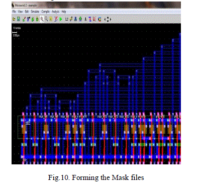
| A delay buffer based on the proposed techniques have designed and simulated. The tool used is Micro wind 3.1 for the backend and for power synthesis, Altera Quartus II 10.0 is used. |
 |
 |
POWER ANALYSIS |
 |
| Comparison power analysis using Micro wind 3.1 |
CONCLUSION |
| In this paper, we presented a low-power delay buffer architecture which adopts several novel techniques to reduce power consumption. The ring counter with clock gated by the C-elements can effectively eliminate the excessive data transition without increasing loading on the global clock signal. An-other gated-demultiplexer tree and a gatedmultiplexer tree are used for the input and output driving circuitry to decrease the loading of the input and output data bus. Measurement results indicate that the proposed architecture consumes less than the conventional architecture that measured in Back End tool. |
FUTURE ENHANCEMENT |
| This low power circuit design is used in portable multimedia and wireless communication devices. More power reduction can be achieved by considering the memory section. Backend by using Micro wind 3.1 The table gives the comparison result between buffer using gated techniques and ring counter with DET flip flop for addressing and the buffer that uses binary counter for addressing. Thus, the proposed buffer consumes less power. |
References |
|