International Journal of Advanced Research in Electrical, Electronics and Instrumentation Engineering
ISSN ONLINE(2278-8875) PRINT (2320-3765)
ISSN ONLINE(2278-8875) PRINT (2320-3765)
G.S.Arun kumar and Kiruthiga.S
|
| Related article at Pubmed, Scholar Google |
Visit for more related articles at International Journal of Advanced Research in Electrical, Electronics and Instrumentation Engineering
A single phase multilevel inverter for dc to ac conversion is developed with minimum number of power electronic devices and isolated DC sources and implemented using FPGA. The total harmonics of the output waveform is reduced by increasing the switching modes with reduced devices. The H-Bridge multilevel inverter has two inverters connected in cascade. The lower inverter is capable of developing a multilevel output and another inverter develops two-level output. Both the inverters operate at different frequency to produce multilevel output. The H-Bridge multilevel inverter has been analyzed in asymmetric conditions. The project work to be proposed is to reduce total harmonic distortion with less number of devices. By increasing the voltage levels at the output, the harmonics of the output waveform can be reduced and made negligible. The topology also produces minimum switching losses compared to the existing methods. The voltage rating of the upper H bridge inverter switches and auxiliary switches in the lower H bridge inverter becomes smaller and smaller compared to the output voltage when the number of levels is increased.The hybrid modulation algorithm is simulated using MATLAB/Simulink. The VHDL code for each of this topology was written and synthesized using Xilinx ISE software. Behavioral Simulation was performed on the architecture and after verifying the results this VHDL code was downloaded to SPARTAN 3A DSP board.
Keywords |
| Field Programmable Gate Array(FPGA),Direct Current(DC),Very High Speed Description Language(VHDL). |
INTRODUCTION |
| During the last few decades, technological improvement in power electronic devices and increasing demand for energy have contributed to quick development of power generation based on renewable energy sources. Photovoltaic (PV), wind and fuel cell (FC)-based renewable energy technologies are paying attention among the researchers over the globe[1-5]. One of the misfortunes focused in the research is the limitation of power electronic switches. If the power electronic devices which can withstand high voltage are used in the inverter,then their switching frequency is restricted automatically. Hence, the device voltage must be diminished to use reckless switching devices. A multilevel inverter can reduce the device voltage and the output harmonics by increasing the number of output voltage levels . This is achieved by increasing the number of isolated DC sources which increases the number of output voltage levels. But this makes the system complex.Booster circuits are also needed for some applications which make the system further more complex. |
| In recent years, solar energy is one of the most important alternative energy sources that has been gaining increased attention. Solar energy has the benefits of no pollution, low maintenance cost and no noise. The conversion of solar energy into electrical energy has been increasing in the past, and a more significant increase is expected in the near future, both for grid-connected and stand-alone applications, due to the saving of the installation cost and the increasing of the energy conversion efficiency of photovoltaic (PV) modules by the results of the advanced material development for PV modules. The optimal DC energy generated from PV modules can be converted to the AC energy and supplied to load or the utility grid by the interfacing of the power converters with the renewable energy sources and loads. The power converters can be controlled by the computation tracking algorithms to operate at the maximum power point (MPP) of the PV modules for exploiting the extracted energy. |
RELATED WORK |
| In single-phase multi-level inverters, the most widely used techniques are cascaded H-bridge (CHB), diode-clamped and capacitor-clamped types . In addition, many more techniques also exist . CHB single-phase inverters are widely used because of their modularised circuit layout and simplicity . A variety of modulation techniques can be applied to CHB inverters. By increasing the number of CHBs, the number of levels in CHB inverters increases. Generally if the number of output voltage levels is increased, then the number of power electronic devices and the number of isolated DC sources is also increased. This makes a CHB inverter further complex. |
| A multilevel inverter with minimum number of power electronic switching devices is proposed which is a modified version of the multilevel inverter using series/ parallel conversion of DC sources (MLISPC) an auxiliary circuit comprising of four diodes and a switch is introduced instead of series/parallel switches of the inverter found in MLISPC[8]. However, only two isolated voltage sources are needed to output the same number of voltage levels compared to conventional CHB inverters and MLISPC.But switching the voltage sources in parallel and series manner makes the circuit still complex. The proposed multilevel inverter topology can be extended for the application of grid connected PV systems, hybrid electric vehicles etc. |
CIRCUIT TOPOLOGY |
| Fig.1 shows the circuit configuration of the proposed cascaded H bridge multilevel upper inverter. |
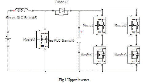 |
| Capacitor sources may either be independent or dependent on each other. The magnitude of each voltage sources in the lower H bridge is two times the magnitude of upper H bridge voltage source. The lower H bridge of MLISPC is interchanged with the one developed in [9]. |
| When the conventional CHB inverter is driven by the hybrid modulation method, 12 switching devices are needed for 11 levels and 16 switching devices are needed for 15 levels. On the other hand, the proposed inverter requires 12 devices for 11 levels and 14 devices for 15 levels. When the ratio of the voltages of the sources is 1 : 3 is assumed, the proposed inverter requires 11 devices for 15 levels and 14 devices for 21 levels which is in the ratio of 1:4. When an inductive load is connected, the output current lags behind the output voltage. Therefore, a state is achieved when the direction of the current becomes reverse to the power sources. On the other hand, when a resistive load is connected, the output current phase is accorded with the voltage phase.Hence,both are connected at the output to overcome the laggings behind one another. |
| Fig.2 shows the lower inverter and the cascaded configuration of both inverters give the final result. |
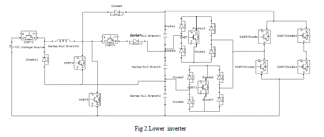 |
| Using this proposed circuit configuration, the lower H bridge inverter outputs Vlow = 2n + 1 levels, whereas the upper H bridge outputs Vup = vdc0. The proposed inverter outputs 4n + 3 levels by Vlow + Vup or Vlow − Vup. Here, n is the number of capacitor sources in the lower H bridge inverter. |
AVOIDANCE OF VOLTAGE BALANCING PROBLEM |
| Applications of Multi Output Boost (MOB) DC–DC converter is the circuit used for boosting and regulating the low and variable output voltage of renewable energy for the DC link of grid connected systems, based on multilevel inverters . Hence the MOB DC–DC[11,12] converter serves for two purposes, they are |
| 1. for boosting low output voltage of PV array or FC stacks to a desired value; |
| 2. balancing of DC link capacitors. |
PWM MODULATION TECHNIQUE |
| The technique used here determines the switching function to obtain a output of 11 levels in the proposed inverter.The general reference waveform is given as |
 |
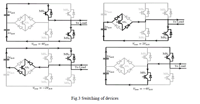
| Fig.3 shows various switching of auxiliary switches to control the output of the switching devices. |
 |
| It is necessary to find out the number of auxiliary switches required for an N-level inverter |
| NAS = ((N - 11)/4)+ 1 |
| where N = 11, 15, 19, 23, . . |
| The modulation index Ma of the proposed N-level inverter is defined as |
| Ma=Apr/MApc |
| where M= (N − 1/2), N = 11, 15, 19, 23, … etc. |
| Where APr represents the peak value of the modulating or reference wave and Apc represents the peak-to-peak value of the carrier (triangular) wave. |
COMPARISON BASED ON VOLTAGE RATING OF THE DEVICES |
| The device rating of the switching devices should be selected sensibly in the recommended inverter, because the voltage rating of each device is different. In the 11-level topology of the proposed inverter, it requires only one auxiliary switch, in this case the auxiliary switch voltage will jump between 0 and (Vdc/2), where Vdc is the input DC source voltage of lower inverter. This is because total voltage of Vdc is divided into two by using two capacitors that is, (Vdc/2) each. Hence, the auxiliary switches have to block the capacitor voltage which is (Vdc/2). In 15-level inverter topology, it requires two auxiliary switches. The entire voltage Vdc will be divided into three-by-three capacitors that is, (Vdc/3) across each. So, the two auxiliary switches voltage will jump between 0 and (2Vdc/3). Further, in the case of 19-level inverter, it requires three auxiliary switches.The first and last auxiliary switch voltages will jump between 0 and (3Vdc/4) and the middle auxiliary switch voltage will jump between 0 and (2Vdc/4). Similarly, for other levels of inverters, the first and last auxiliary switch voltage jumps between 0 and ((n − 1)Vdc/n), whereas the other auxiliary switch voltage jumps between 0 and ((n − 2) Vdc/n), ((n − 3)Vdc/n)… and so on. |
RESULTS |
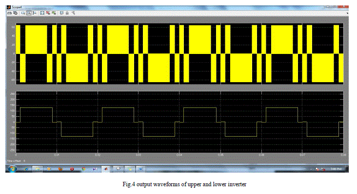
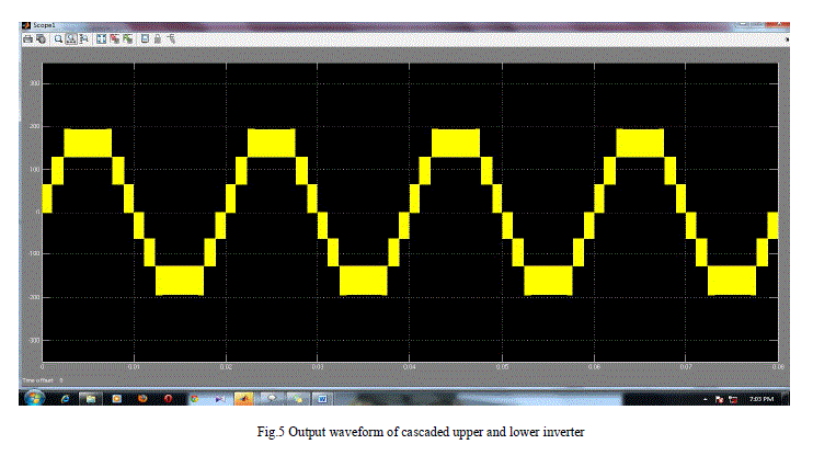
| The gate driving signal is developed by using field programmable gate array (FPGA)-Xilinx SPATRAN 3A DSP. The software used to develop programs for SPATRAN 3A DSP are Xilinx ISE Design Suite and Multisim. The upper inverter is operated at high switching rate that is equivalent to the carrier frequency (i.e. 10 kHz), whereas the lower inverter is operated at low frequency (nearly equal to the fundamental frequency i.e. 50 Hz). Any reduction in the modulation index further will reduce the number of voltage levels at the load end. For example when A = 2 that is, Ma = 0.28, voltage level at the load becomes five and so on. In order to validate the proposed multilevel inverter fed from multioutput DC–DC boost converter, a step change in the reference values of the lower DC link capacitors were given at 0.5 s (i.e. from 50 to 100 V).Fig.4 and Fig.5 shows the output waveforms of upper inverter, lower inverter and cascaded output(almost sine wave with less harmonics). Fig.1 and Fig.2 shows the connected circuit of upper and lower inverter.Fig.3 shows the switching of devices to get proper output of lower inverter.Fig.4 shows the results of the output of lower and upper inverter. Fig.5 shows the final output which is almost sinewave. |
 |
 |
 |
| WOF – without filter |
| WLCF – with LC filter |
CONCLUSION |
| Multilevel inverters offer enhanced output waveforms with minimum THD. This paper has presents a novel singlephase multilevel inverter with reduced switching devices and isolated DC sources. Simulations are carried out in MATLAB/Simulink and implemented in real-time using FPGA board. The capacitor voltage balancing problem is avoided for higher levels by using booster circuit.A generalised switching algorithm that can be used for any number of levels can be designed.. The modulation waveform and the harmonic analysis are also presented for various values of modulation indices. By properly adjusting the modulation index, the required number of levels of the inverter output voltage can be achieved.The simulation and experimental results match perfectly with each other. This proposed inverter system offers the advantage of reduced switching devices and isolated DC sources when compared to the conventional CHB and MLISCP for the same number of output levels. Also, high-frequency switching devices are operated at low voltage and low-frequency devices are operated at high. Thus, it can be concluded that the proposed novel multilevel inverter can be used for medium- and high-power applications. |
References |
|