International Journal of Advanced Research in Electrical, Electronics and Instrumentation Engineering
ISSN ONLINE(2278-8875) PRINT (2320-3765)
ISSN ONLINE(2278-8875) PRINT (2320-3765)
| Md. Jahid Hasan, Md. Hasibul Islam and Qazi Tareq Undergraduate student, Dept. of EEE, AIUB, Dhaka, Bangladesh |
| Related article at Pubmed, Scholar Google |
Visit for more related articles at International Journal of Advanced Research in Electrical, Electronics and Instrumentation Engineering
The conventional ac-dc converters for energy harvesting system with diode rectifiers suffers considerable voltage drop results increase in power loss of circuitry and complexity. The bridgeless boost rectifier which is a unique integration of boost and buck boost to condition the positive and negative half portions of the input ac voltage, respectively. Such a single stage ac-dc converter has been designed and simulated using MATLAB/SIMULINK at 50-kHz switching frequency. The boost and buck-boost topologies could share same inductor and capacitor to meet the miniature size and weight requirements. The input ac voltage with 10V amplitude is rectified and stepped up to 30V dc. Detailed design guidelines are provided with the purpose of minimizing the size, weight, and power losses.
Keywords |
| Ac/dc conversion, boost, bridgeless, buck-boost, energy harvesting. |
INTRODUCTION |
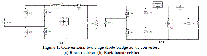
| In energy harvesting systems, power electronic circuit forms the key interface between transducer and electronic load, which might include a battery. A compact, highly efficient power management circuit is as important as the harvester itself. A complete energy harvesting solution obviously requires the harvester for mechanical to electrical energy conversion, but also application specific power management circuitry to perform ac/dc rectification, voltage/current boost, voltage/current regulation, and other power management functions.Conventional ac–dc converters for energy harvesting and conditioning usually consists of two stages. A diode bridge rectifier typically forms the first stage, while the second stage is a dc–dc converter to regulate the rectified ac voltage to a dc voltage (in Fig. 1). This arrangement of two stage power conversion has several disadvantages: |
| 1) Diode voltages in a bridge rectifier are difficult to overcome for low input voltage. |
| 2) Diode losses are increased, as input current is much higher than output current. |
| 3) A rectifier offers a nonlinear load, which makes the converter unsuitable for energy harvesting. |
| To overcome these drawbacks, CMOS diodes with low voltage drops are investigated in the bridge rectifiers, to substitute conventional p-n junction diodes. Such diodes include1) diode-connected passive MOSFET, which adopts threshold voltage cancellation techniques and 2) MOSFET, which is actively controlled by a comparator. |
| In the either case, the low-voltage-drop diode techniques require either additional bias networks or external comparators. Thus, both the complexity and the power loss of the circuitry would increase. |
 |
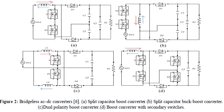
| Another approach to maximize the conversion efficiency in low-voltage rectification is to use bridgeless direct ac–dc converters. Those topologies either use bidirectional switches and split capacitors, or two parallel dc–dc converters to condition positive and negative input voltages separately. For the split-capacitor topologies [in Fig. 2(a)–(c)], due to the low operation frequency, the capacitors have to be large enough to suppress the voltage ripple under a desired level. The increased size and number of energy storage components make those topologies impractical due to the size limitation of energy harvesters. On the other hand, the split capacitors could be eliminated by using two synchronous MOSFETs [in Fig. 2(d)]. However, the additional switches would incur extra switch loss and driving circuit dissipations. |
 |
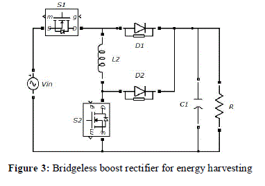
| Step up the input voltage with a reverse polarity; hence, it is an appropriate candidate to condition the negative voltage cycle. Beside the boost and buck – boost topologies, it could share the same inductor and capacitor to meet the miniature size and weight requirements. A new bridgeless boost rectifier, shown in Fig. 3, which is a unique integration of boost and buck-boost converters, is presented in this paper. When the input voltage is positive, S1 is turned ON and D1 is reverse biased, the circuitry operates in the boost mode. As soon as the input voltage becomes negative, the buck boost mode starts with turning ON S2 and reverse biasing D2. MOSFETs with bidirectional conduction capability work as two-quadrant switches to ensure the circuitry functionality in both positive and negative voltage cycles. This topology was introduced in [10] for piezoelectric energy harvesting applications. |
 |
| The circuit operation modes are described in Section 2. In Section 3, the design procedures and guidelines are discussed. Section 4 addresses the simulation results. Section 5 presents the conclusions. |
PRINCIPLE OF OPERATION |
| The power electronics interface (PEI) is employed to supply constant voltage and to deliver power to the load. In order to facilitate and simplify analyses, it is assumed that the input impedance of the PEI is significantly larger than the internal impedance of energy harvesting device. The induced voltage could be assumed to be a low amplitude sinusoidal ac voltage source. In this paper, a 10-V, 50-Hz sinusoidal ac voltage source is adopted to emulate the output of the energy harvester. |
| The DCM operating modes of the proposed boost rectifier are shown in Fig. 4. Each cycle of the input ac voltage can be divided into six operation modes. Modes I–III illustrate the circuit operation during positive input cycle, where S1 is turned ON while D1 is reverse biased. The converter operates as a boost circuit during Modes I–III, while switching S2 and D2. The operation during negative input cycle is demonstrated in Modes IV–VI, where S2 is turned ON while D2 is reverses biased. In these modes, the converter operates similar to a buck-boost circuit. |
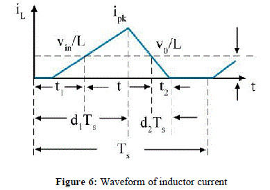
| Mode I: This mode begins when S2 is turned ON at t0. The inductor current is zero at t0. The turn on of S2 is achieved through zero current switching (ZCS) to reduce switching loss. Inductor L is energized by the input voltage as both S1 and S2 are conducting. Both diodes are reverse biased. The load is powered by the energy stored in the output filter capacitor C. |
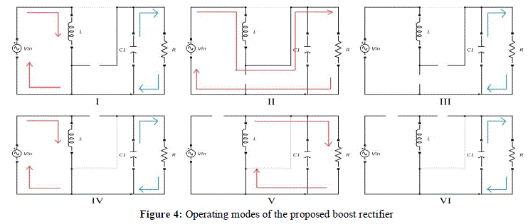 |
| Mode II: S2 is turned OFF at t1, where t1 − t0 = d1Ts, d1 is the duty cycle of the boost operation, and Tsis the switching period. The energy stored in the inductor during Mode I is transferred to the load. The inductor current decreases linearly. During this mode, switching loss occurs during the turn on of diode D2. |
| Mode III: D2 is automatically turned OFF as soon as the inductor current becomes zero at t2 (t2 − t1 = d2Ts). This avoids the reverse recovery loss of diode. The load is again powered by the stored energy in the capacitor. The converter would return to Mode I as soon as S2 is turned ON, if the input voltage is still in positive cycle. |
| Mode IV: During the negative input cycle, Mode IV starts as soon as S1 is turned ON at t_0. ZCS condition can also be achieved by ensuring the converter operation in DCM. The energy is transferred to the inductor L again, while the output filter capacitor C feeds the load. |
| Mode V: At t_1, S1 is turned OFF, where t_1 − t_0 = d_1 Ts, d_1 is the duty cycle of the buck-boost operation. Theenergy stored in the inductor during Mode IV is transferredto the load. The inductor current decreases linearly. Duringthis mode, switching loss occurs during the turn on of thediode D1. |
| Mode VI: When the inductor current decreases to zero at t_2 (t_2 − t_1 = d_2Ts), D1 is turned OFF at zero current. The load is continuously powered by the charge stored in the output capacitor. The converter would return to Mode IV as soon as S1 is turned ON, if the input voltage is still negative. |
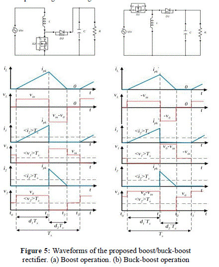 |
| According to the analyses of operation modes, the switches are turned ON with ZCS and the diodes are turned OFF with ZCS. Due to the DCM operation, the input current sensor can be eliminated and switching loss can be reduced. Moreover, the control scheme of DCM operation is relatively simpler. Since the circuit size can be reduced and the efficiency can be enhanced, DCM operation is more suitable than continuous conduction mode (CCM) operation. |
DESIGN PROCIDURE |
| In order to design the circuit, several assumptions are made during one switching cycle. |
| The output filter capacitor C is large enough to keep the output voltage V0 constant. |
| The input is a sinusoidal voltage source. The switching frequency is much higher than the input voltage frequency. During each switching cycle, the input voltage could be treated as a constant voltage source and be expressed as (1), where Vin is the period of input voltage |
 |
 |
| fs - Switching frequency |
| Ts - Switching cycle |
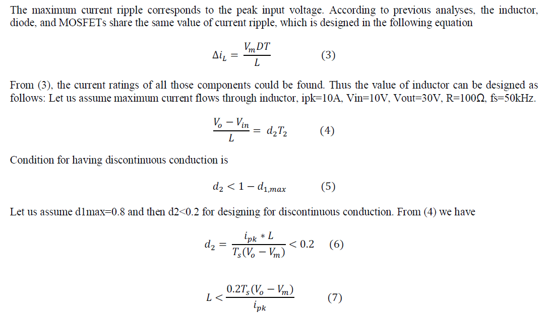
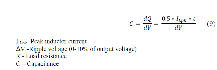
| The voltage ratings of the MOSFETs and diodes are normally chosen higher than Vo with an appropriate margin for safe operation. The turn-on resistances of MOSFETs and the forward voltage drop of diodes are the major components, which impact the efficiency. The output filter capacitance should be selected in order to reduce the ripples presented in the output voltage. The value of capacitance is calculated from the graph. |
 |
| Both the boost and buck-boost operations of the converter From Fig. 3, |
 |
 |
SIMULARION RESULTS |
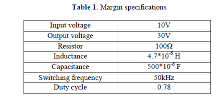
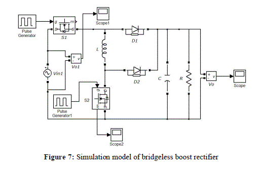
| Simulation circuit for a bridgeless boost rectifier with input voltage 10V and output voltage of 30V is shown in Fig.7. The circuit components are selected in according to the relation (1)-(9) and are listed in the table 1. |
 |
| Closed-loop voltage control successfully stabilizes the duty cycle at 0.78 at the steady state. |
 |
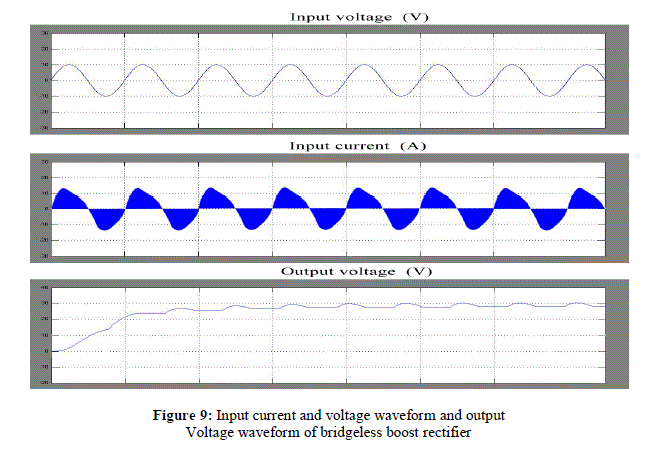
| The bridgeless boost rectifier was simulated using MATLAB/SIMULINK and the resulting waveforms are as shown below. |
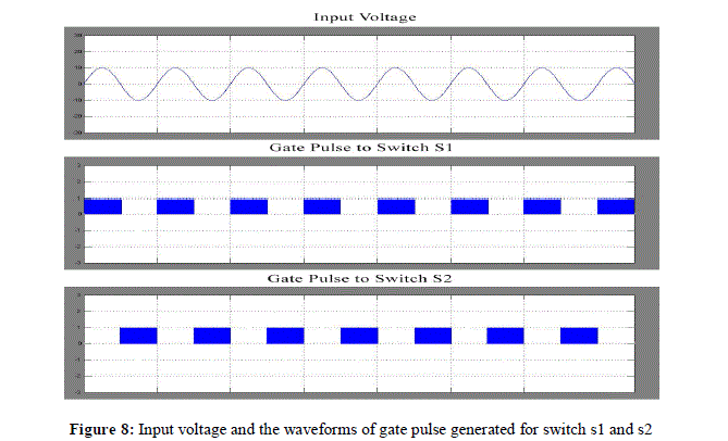 |
| During the positive input cycle, S1 is turned ON, while S2 is driven by the boost control scheme. When the circuit operates in the negative input cycle, S2 is turned ON, while S1 is controlled under the buck-boost conditioning strategy. As seen from Fig. 9, the output voltage is regulated at30-V dc with approximately 0.2 V (i.e., 6%) voltage ripple. |
 |
CONCLUSION |
| The bridgeless boost rectifier was simulated using MATLAB/SIMULINK. The topology combines a boost converter and a buck-boost converter to condition the positive input cycles, respectively. Only one inductor and one filter capacitor are required in this topology. The topology successfully boosts the 10V, 50Hz ac to 30Vdc. The output voltage regulated to 30V through closed loop voltage control. In comparison to state-of-art bridgeless rectifiers, this study employs the minimum number of passive energy storage components, and achieves the maximum conversion efficiency. Te future research will be focused on investigating and designing for much more voltage for various other applications and the distortion in the input current can be reduced by designing a suitable circuit. |
References |
|