International Journal of Advanced Research in Electrical, Electronics and Instrumentation Engineering
ISSN ONLINE(2278-8875) PRINT (2320-3765)
ISSN ONLINE(2278-8875) PRINT (2320-3765)
Anoop D Nath1 and K Radhakrishnan2
|
| Related article at Pubmed, Scholar Google |
Visit for more related articles at International Journal of Advanced Research in Electrical, Electronics and Instrumentation Engineering
In this work, a single-switch resonant boost converter with an energy-blocking diode was proposed for use in a solar energy generation system. The structure of the proposed converter is simpler and cheaper than other resonant power converters, which require numerous components. The proposed single-switch resonant power converter offers the advantages of soft switching, reduced switching losses, and increased energy conversion efficiency. This circuit topology integrates a single-switch resonant converter with zero-voltage-switching (ZVS) with an energyblocking diode with zero-current-switching (ZCS). The energy blocking diode with a direct current (DC) output filter filters the output stage of the single-switch resonant converter. Only one active power switch is used for power energy conversion to reduce the cost of active power switches and control circuits. Simulation results demonstrate a satisfactory performance of the proposed topology, which is especially suited to the energy conversion applications in photovoltaic energy generation systems.
Keywords |
| Resonant Power Converter, Photovoltaic Energy Generation, Soft Switching. |
INTRODUCTION |
| The global demand for electric energy has continuously increased over the last few decades. Energy and the environment have become serious concerns in today's world. Nowadays, most power that is used to meet our daily needs is obtained from fossil fuels. Owing to increases in consumption, fossil fuel sources may be exhausted in the near future. Besides, combustion of fossil fuels results in a serious threat of global warming. As people are much concerned with the fossil fuel exhaustion and the environmental problems caused by the conventional power generation, renewable energy sources and among them fuel cells, photovoltaic panels and wind-generators are now widely used ([1],[2]). Among all renewable energy resources, photovoltaic (PV) power generation systems have been regarded as the most promising future sources of energy because of their advantages, such as the absence of a need for fuel and the associated cost saving, low maintenance, lack of noise, pollution-free, nonradioactive and inexhaustible ([3]-[5]). |
| If the DC output of photovoltaic energy generation systems is directly connected to a battery energy storage system (BESS), then the output voltage of the DC output source of the photovoltaic energy generation system will be fixed to the voltage of the BESS, so the photovoltaic energy generation system cannot always operate optimally. Hence, a DC/DC interface must be installed between the photovoltaic energy generation system and the BESS to ensure that the photovoltaic energy generation system always operates at its optimum operating points. The DC/DC interface is generally a power converter operated with one or more power semiconductor switches. The simplest method for controlling these switches is PWM technigue. Conventional power converters uses hard switching in which the voltage across or current through the switch is abruptly altered to control power flow ([6],[7]). Eventhough hard switching has advantages such as simplicity and ease of control it can’t be used for high switching frequencies, as the converter switching losses increases with increase in switching frequency, it also increases stress on the device and system EMI. |
| Inorder to reduce high voltage and current stress problems energy conversion using resonant converters is gaining more popularity ([8],[9]). The basic requirements of resonant converters are their small size and high efficiency. A high switching frequency is required to achieve small size. However, the switching loss increases with the switching frequency, reducing the efficiency of the resonant converters. To solve this problem, some soft switching approaches must be used at high switching frequencies[10]. |
| A single-switch resonant boost converter for photovoltaic energy generation system is discussed in this paper. The circuit topology integrates a single-switch resonant power converter with Zero Voltage Switching (ZVS) of active power switch and an energy blocking diode with Zero Current Switching (ZCS). This reduces the switching losses when operated with higher switching frequency and as a result the conversion efficiency is improved. The use of proposed resonant boost converter in photovoltaic energy generation system provides many advantages, such as a less number of components, ease of control, low cost and high power density. The proposed topology is simulated using PSIM and the results are presented to verify the operation of the converter. |
OPERATING PRINCIPLES OF THE PROPOSED RESONANT BOOST CONVERTER |
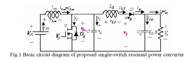
| The work proposes a single-switch resonant boost converter which can be implemented in photovoltaic energy generation systems. Fig.1 shows the basic circuit diagram of proposed resonant converter. The converter consist of an active power (MOSFET) switch operated with ZVS and an energy blocking diode operated with ZCS. Other components include a choke inductor Lm , a shunt capacitor C, a resonant inductor Ls, an energy-blocking diode D, and a filter capacitor Co. The capacitance Co and the load resistance R together form a filter, which reduces the ripple voltage. |
 |
| A. Modes of Operation |
| The operation of the converter can be explained with the help of waveforms shown in Fig.2. One switching cycle is divided into six modes which can be explained as follows. |
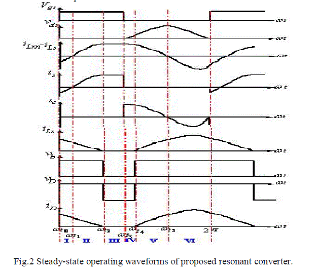 |
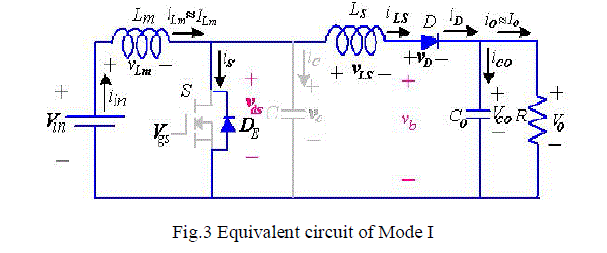
| 1. Mode I ( ωt0 – ωt1 ) : In this mode the active power switch S is off. The switch S must be turned at zero voltage. Otherwise the energy stored in the active power switch is dissipated in the active power switch S, to prevent this situation the antiparallel diode DE must conduct before the power switch is turned on. When the capacitor voltage vC falls to zero, a turn on signal is applied to the gate of the active power switch. In this mode both the anti-parallel diode DE and the energy blocking diodes D are forward biased. This mode ends when the anti-parallel diode DE is reverse biased by a positive current iLm-iLs. |
 |
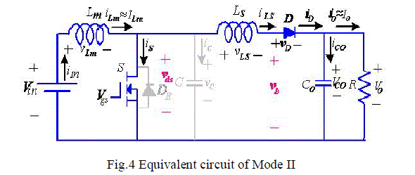
| 2. Mode II ( ωt1 – ωt2 ) : The equivalent circuit of this mode is shown in Fig.4. In this mode the switch S is in the ON state. The inductor current iLm increases continuously. In this mode the anti-parallel diode DE is reverse biased and the current iLm - iLs flows through switch S. As a result the voltage across the capacitor C drops to zero. The energy blocking diode is forward biased and the resonant current iLs flows through it. Mode II ends when the inductor current iLs falls to zero. |
 |
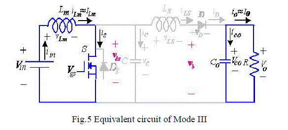
| 3. Mode III ( ωt2 – ωt3 ) : In this mode the switch S remains in the on state and the choke inductor current iLm continuously increases and inductor current iLs falls until it reaches zero. In this topology the DC input is never connected directly to the output load. When the switch is turned on energy is stored in the choke inductor Lm and is transferred to the output load when switch is turned off. This mode is exited when the power switch S is turned off. |
 |
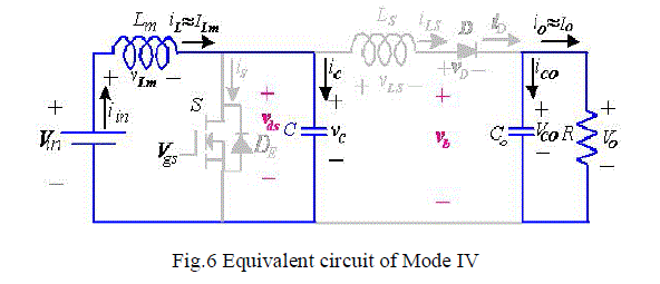
| 4. Mode IV( ωt3 – ωt4 ) : This mode starts when the power switch is turned off. In this mode iC = iLm , and it flows through capacitor to charge C, transferring the energy from DC input source to capacitor C. In this mode the output power of load resistor is supplied by the output capacitor Co. It is clear from Fig.2 that the active power switch is turned off under ZVS condition. |
 |
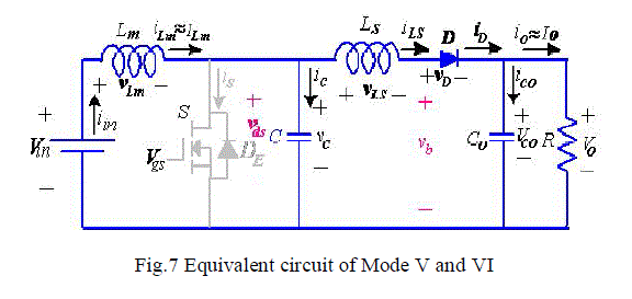
| 5. Mode V ( ωt4 – ωt5 ) : In this mode the switch S is in the off state. The energy-blocking diode D is forwrd biased by the positive inductor current iLs , which results a resonant stage between inductor Ls and capacitor C. The equivalent circuit of this mode is shown in Fig.7. |
| 6. Mode VI ( ωt5 – ωt6 ) : The mode begins when capacitor voltage vC resonates from negative values to zero. Before the cycle of the resonant inductor current iLs oscillation ends, the active power switch S is kept off condition, constraining the positive current to flow continuously through the energy-blocking diode D. In addition to the active power switch, the energy-blocking diode in the proposed converter is also commutated under soft-switching. When the driving signal Vgs again excites the active power switch S, this mode ends and the operation returns to mode I in the following cycle. |
 |
SIMULATION RESULTS |
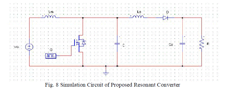
| The proposed single-switch resonant converter is simulated using PSIM to demonstrate the relevant theory. Instead of the photovoltaic system a 12V DC input is given as the input to the converter. Fig. 8 shows the simulation model of the converter in PSIM . |
| To realize ZVS operation of the active power switch and ZCS operation of the energy-blocking diode of the converter, the switching frequency must satisfy fs < fo . The simulation was performed under the following conditions; switching frequency fs = 70kHz, resonant frequency fo = 86kHz, duty cycle k = 0.63 and output voltage Vo = 24.0V. To reduce input current ripple and maintain stability of the output voltage, the low-pass filters at the input and output terminals, which use a choke inductor and an electrolytic capacitor, are set to Lm = 8mH and Co = 220μF, respectively. The low-pass filter is designed to be small, light, and low-cost. Under the aforementioned operating conditions, the two parameters of the single-switch resonant power converter are C = 0.18μF and Ls = 19μH. |
 |
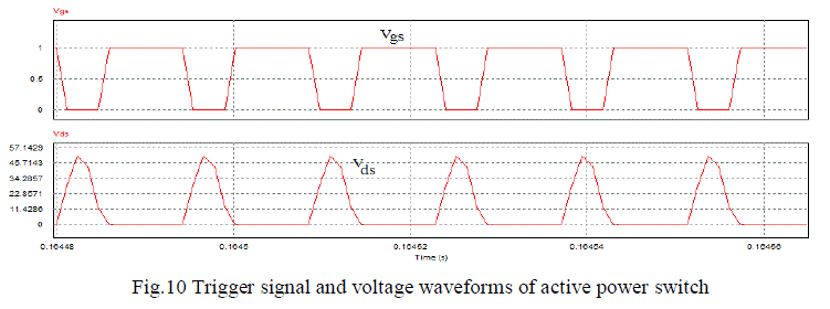
| The following results were obtained from the simulation with above parameters. Fig.10 shows the waveforms of the active power switch S, where vgs represents the trigger signal on active power switch S, and vds represents the voltage across the active power switch S. |
 |
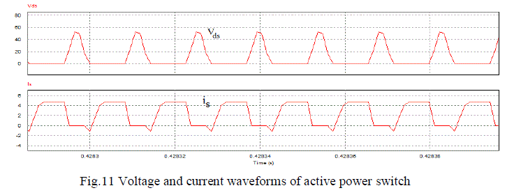
| Fig.11 depicts the voltage and current waveforms of the active power switch S. Evidently, the active power switch is operated with ZVS. |
 |
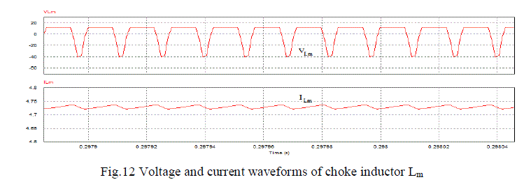
| Fig.12 displays the voltage and current waveforms of the choke inductance Lm at the input terminal. The choke inductance Lm is suffciently large that the input current iLm is almost constant. |
 |
 |
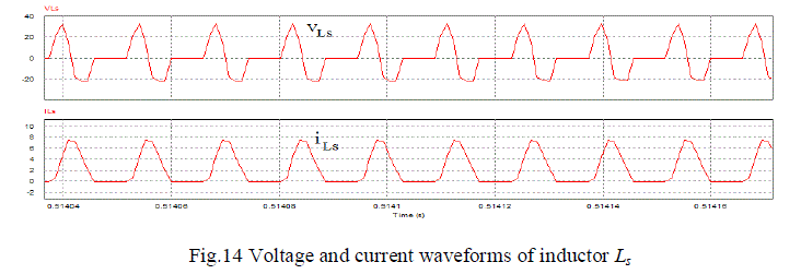
| Fig.14 plots the voltage waveforms of the resinant inductor vLs and the current waveform of resonant inductor iLs. |
 |
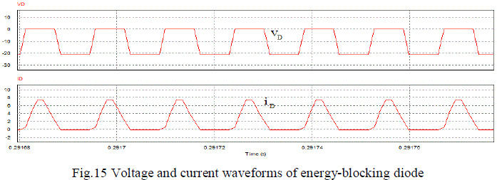
| Fig.15 illustrates the voltage and current waveforms of the energy-blocking diode. This figure reveals that this diode is operating under the ZCS condition, which can reduce the switching loss and increase the energy conversion effciency. |
 |
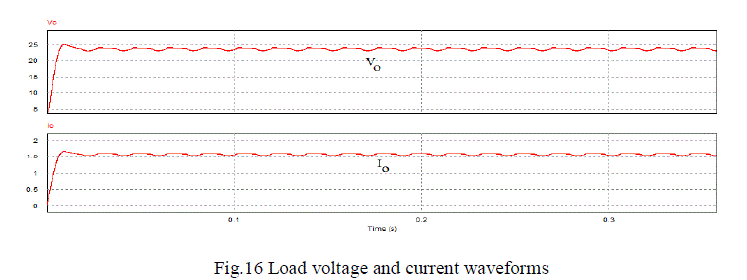
| Figure 16 gives the output voltage and current waveforms of the load. The simulated effciency is found to be 94.4%. |
 |
CONCLUSION |
| In this work, a highly effcient single-switch resonant boost converter with an energy-blocking diode was designed for use in a solar energy generation system. The structure of the proposed converter is simpler and cheaper than other resonant power converters, which require numerous components. The developed single-switch resonant power converter offers the advantages of soft switching, reduced switching losses, and increased energy conversion effciency. The perfomance of the proposed converter is analysed with the help of simulation results and the simulated effcency of the converter is found to be 94.4%. If the converter is connected to a PV energy generation system with Constant Voltage MPPT control, the system can be used as a battery charger without any feedback controllers as the output voltage of the converter remains constant. |
References |
|