International Journal of Advanced Research in Electrical, Electronics and Instrumentation Engineering
ISSN ONLINE(2278-8875) PRINT (2320-3765)
ISSN ONLINE(2278-8875) PRINT (2320-3765)
R.Ramya1,V.Saranya1 and Y.Vivekananth2
|
| Related article at Pubmed, Scholar Google |
Visit for more related articles at International Journal of Advanced Research in Electrical, Electronics and Instrumentation Engineering
An explicit pulsed dual edge triggered sense amplifier flip flops (DET-FF).In this dual edge triggered sense amplifier flip flop is used for low–power consumption and high performance application. By incorporating the dual edge triggering mechanism, the dual edge triggered flip flop is able to achieve low power consumption that has minimum delay. Clock gating is a popular technique used in many synchronous circuits; hence, the power dissipation is very much reduced. Reducing dynamic power reduction. Clock gating saves power by adding more logic gates in the circuit. It can be used in various applications like digital VLSI clocking system, buffers, registers, microprocessors etc.
Keywords |
| Clock pulse gating,high performance,low power,delay,pulse dual edge triggered, sense amplifier flip flop. |
INTRODUCTION |
| In many digital very large scale integration (VLSI) design, which consists of the clock distribution network and timing elements, is one of the most power consumption. Flip- flops are critical timing elements in digital circuits which have a large impact on circuit speed and power consumption. The performance of the Flip- Flop is an important element to determine the performance of the whole synchronous circuit. |
| In this dual edge triggered sense amplifier as developed from single edge triggered sense amplifier flip flops. At each rising or falling edge of a clock signal, the data stored in a set of flip-flops is readily available so that it can be applied as inputs to other combinational or sequential circuitry. Such flip- flops that store data on both the leading edge and the trailing edge of a clock pulse are referred to as double-edge triggered flip-flops otherwise it is called as single edge triggered flip-flops. |
| The dual edge triggering is a very important technique is to reduce the power consumption in the clock distribution network. In this dual edge triggering is to introduce the clock gating. In this clock gating with clock storage element is to reduce the dynamic power. Two types of clock gating are used in the dual edge triggering mechanism. These are latch free clock gating and latch based clock gating. When technology scales down, total power dissipation will decrease and at the same time delay varies depends upon supply voltage, threshold voltage, oxide thickness. |
DUAL EDGE TRIGGERED FLIP FLOP |
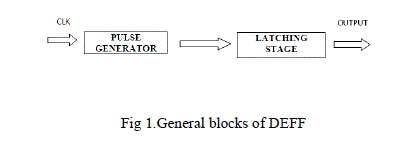
| The dual edge triggered flip flops have two stages. These are pulse generator stage and latching stage. If the clock pulse as the input of the pulse generator. It produces the triggering pulse signal. Latching stage as generate the output pulse signal. |
| In this dual edge triggering flip flop used two types of clock gating. These are latch based clock gating and latch free clock gating. The general block is shown in Fig 1. |
 |
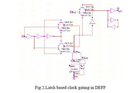
| The schematic diagram of the dual edge triggered flip flop in latch based clock gating as shown in figure 2. |
| In this latch based clock gating in DEFF in1 and in 3 has falling we get ‘0’ output. In2 have falling get ‘1’as the output. If the clock as the positive (clk==1) edge clock. The latch based clock gating styles adds a level sensitive latch to the design to holds the enable signal from the active edge of the clock, until the inactive edge of the clock. Since the latch captures the state of the enable signal and holds it until the clock pulse have been generated. The enable signal need only be stable around the rising edge of the clock |
 |
| The schematic diagram of the dual edge triggered flip flop in latch free clock gating as shown in figure 3. |
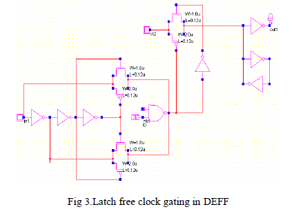 |
| In this latch free clock gating in DEDFF is output initially ‘0’.Then all input we get high output. The latch free clock gating styles uses a simple AND or OR gate and impose a requirement on the circuit that all enable signals be held constant from the active (rising) edge of the clock until the inactive (falling) edge of the clock. In order to avoid truncating the generated clock pulse generating multiple clock pulse where one is required. |
LATCH BASED CLOCK & LATCH FREE CLOCK GATING IN PULSE GENERATOR STAGE |
| In this proposed clock gated flip flop used two types of clock gating. The general schematic is shown in figure 4. |
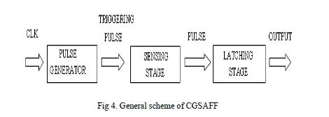 |
| The proposed clock gated sense amplifier flip flop have three stages. These are pulse generator stage, sensing stage and latching stage. Pulsed generator stage as produce the triggering pulse. The sensing stage is to sense the triggering pulse of the signal. The latching stage as to produce the output signal. |
| In order to compare the previous and current input values, X and Y these are the differential inputs. in1, in2, in3, and in4 these are the buffered output. out1, out2, out3 and out4 these are the control signals. If in2 and in4 is different from the output out 1 and out4, X will be pulled up to high and Y pulled down to low.CL as known as the gated clock. At the rising edge of the clock, CL as goes to high and delayed signal CLK3 as goes to low. Therefore transistor and transmission gates are turned on, pulse signal as goes to high. After a short period, transparent window is closed as CLK1 goes to low and CLK 3 as pulled up to high. |
| At the falling edge of the clock, CL as pull down to low and delayed signal CLK3 is high. Once the CLK3 is low, the sampling window is shut down. |
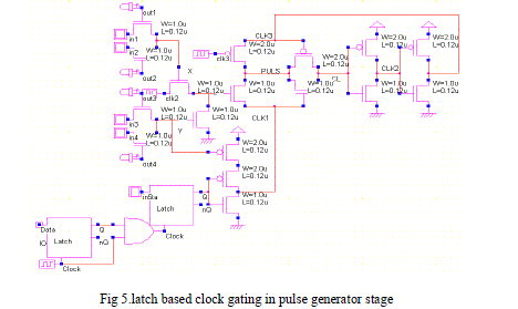
| The schematic diagram of the clock gated sense amplifier flip flops in latch based clock gating in pulse generator stage as shown in fig 5. |
| In this latched based clock gating two latches are connected in series .between these two latches one and gated is connected. For latch input is enable input. In this input is always high. Then another one of the input is data input. Instead of clock replace the latch based clock gating. By using the latch based clock gating we consume the power. |
 |
| The schematic diagram of the clock gated sense amplifier flip flops in latch free clock gating in pulse generator stage as shown in fig 6. |
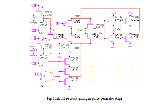 |
| In this latch free clock gating one AND gate is connected instead of the clock pulse. In this AND gate inputs are clock and enable signal. |
| In the evaluation phase ,in1 is low, SB will be set to high, and if in2 is high , RB will be set to high.therefore ,the conditional precharging technique is applied in the sensing stage of the CG-SAFF.two input controlled pmos transistors are embedded in the pre charging paths of the nodes SB and RB. |
| The schematic diagram of the clock gated sense amplifier flip flops in latching stage as shown in fig 7. |
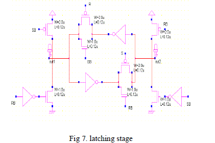 |
| To optain the differential buffered output as to reduce the loading capacitance.By using this latch stage we know the output signal.the clocking stage as used to improve the performance of the CG-SAFF. |
SIMULATION RESULTS |
| The simulation results were obtained from WINSPICE in cmos technology.all the flip flops were designed using chartered semiconductor limited in 0.18umCMOS process technology,at an operating temprature of room temperature and supply voltage as 1.8V. |
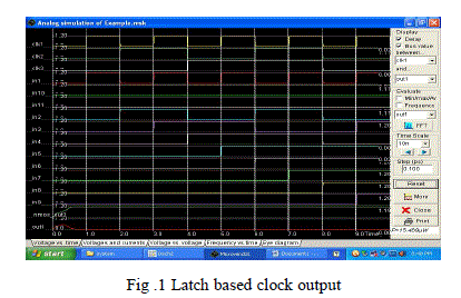 |
| Above figure.1 shows the output of the clock gated flip flops in latch based clock gating. In this technique generate 15.486 uw power. |
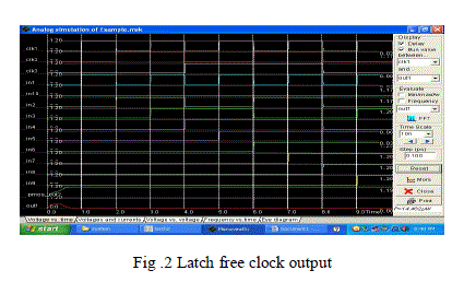 |
| Above figure.2 shows output of the latch free clock gating in clock gated flip flop. In this technique generate 14.46uw power. |
PERFORMANCE COMPARITION |
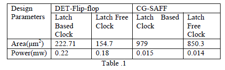
| Table. 1 presents the comparision between the DET-FF and CG-SAFF. Here analyze different designs in the view of total layout area and power consumption |
 |
CONCLUSION |
| This paper presents clock gating sense amplifier flip flops in dual edge triggered flip flops for low power and high performance applications. In this explicit pulsed dual edge triggered flip flops have to achieve power dissipation reduction by incorporating dual edge triggering. Dual edge triggered flip flop is also reduce the latency, the area and saving the power. It can be used in various applications like digital VLSI clocking system, buffers, registers, microprocessors etc. |
References |
|