Wireless technology is emerged has the vibrant research areas in the modern communication industry. The IEEE 802.16e has defined a standard commonly known as mobile WiMAX and emerged as the latest wireless technology that has promised to offer Broadband Wireless Access over long distance. This paper proposes an algorithm on address generation circuitry of Deinterleaver using QPSK and 16-QAM modulation for WiMAX transceiver. The floor function associated with the implementation of FPGA is very difficult in IEEE 802.16e standard. The requirement of floor function can be eliminated by using a simple mathematical algorithm. The main aim of the work is to concentrate on performance improvement by reducing interconnection delay, lesser power consumption, and efficient resource utilization by comparing with prevailing technique.
Keywords |
| Deinterleaver/Interleaver circuit, Wireless systems. |
INTRODUCTION |
| Broadband Wireless Access (BWA) is continuously becoming a more challenging competitor to the conventional
wired last mile access technologies. IEEE has developed standards for mobile BWA (IEEE 802.16e) popularly referred
to as mobile WiMAX [1]. |
| The channel interleaver employed in the WiMAX transceiver plays a vital role in minimizing the effect of burst error.
Memory utilization and frequent memory accesses time are a crucial part of inter leaver design. Basically, the
interleaving technique is to reorder the encoded data such that the adjacent bits can now become nonadjacent which can
help handling the burst error occurring in those channels with memory. Although the basic concept of interleaving is
straight-forward, the way of data reorder can be quite complex. In addition, to reorder a sequence of data requires a
large memory buffer and frequent memory access such that the deinterleaver may become a crucial part of the overall
decoder circuit in both area and power. Therefore, how to design an efficient deinterleaving circuit is very important [2]. |
| In this paper, a novel, less-complexity, high-speed, and efficient resource address generator for the channel
deinterleaver used in the WiMAX transreceiver eliminating the requirement of floor function is proposed. Very few
works related to hardware implementation of the project is used the interleaver/deinterleaver used in a WiMAX system
is available in the literature. The work in [3] demonstrates the grouping of incoming data streams into the block to
reduce the frequency of memory access in a deinterleaver using a conventional lookup table (LUT)- based CMOS
address generator for WiMAX. A low cost and re-configurable architecture for address computation is always
beneficial. IEEE 802.16e [5] called WiMAX is being used in the communication industry with many variants in
channel coding, like different block sizes and different modulation schemes (e.g. BPSK, QPSK, 16 QAM and 64-
QAM). |
| The type of interleaver used here is the block interleaver, in which the data is written sequentially in a memory and
read in a random order after applying certain permutations.. Some work [2] – [4] has been published for the hardware implementation of WiMAX interleaver in different scenarios, but no mathematical formulation has been proposed
behind the implementation. This paper emphasizes on reduction in complexity of the address generation by 2-D
transformation of the original interleaving functions. Software simulation using ModelSim is performed to verify the
functionality of the proposed algorithm and hardware. FPGA implementation results along with their possible
comparison with recent similar work have been made. |
| Use of FPGA‘s embedded multiplier provides performance improvement by reducing interconnection delay,
resource and power consumption compared with a configurable logic block-based multiplier [9]. |
II. RELATED WORK |
2.1 WiMAX CHANNEL INTERLEAVER |
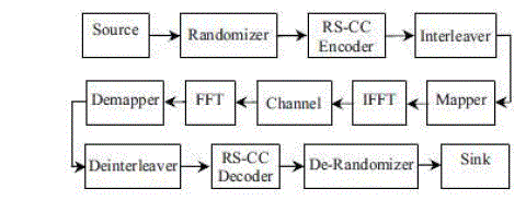
| The blocks of a WiMAX transreceiver are shown in fig.1. The output of source is randomized before being encoded
by two Forward Error Correction (FEC) coding techniques, namely, Reed–Solomon (RS) and Convolutional Coding
(CC). The channel interleaver permutes the encoded bit stream to reduce the effect of burst error. When Convolutional
Turbo Code (CTC) is used for FEC, being used as optional in WiMAX, hence the channel interleaver is not required;
CTC itself includes an interleaver within it [7]. Modulation and construction of the orthogonal multiplexing symbols
are performed by the two subsequent blocks, namely, mapper and Inverse Fast Fourier Transform (IFFT) of Fig.1. In
the receiver end, the blocks are organized in the reverse order to obtain the restoration of the original data sequence at
the output [8]. |
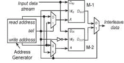
| Two-dimensional block interleaver/deinterleaver structure, is used as a channel interleaver/deinterleaver
in the WiMAX system, is described in fig.2.It consists of two memory blocks, namely, M-1/2 and an address
generator. In block interleaving, when one memory block is being written, the other is read, and vice versa. When
sel =1, write enabled signal WE of M-1 is active. During this time, the input data stream is written in M-1 as it
receives the write addresses. Simultaneously, an interleaved data stream is read from M-2 as it is supplied with the
read addresses. After the memory blocks are written/read up to the desired location as specified by interleaver
depth, the status of sel signal is changed to swap the write/read operation. |
| The block interleaver/deinterleaver exploits different depths ‘Ncbps’ to incorporate various code rates and modulation
schemes for IEEE 802.16e. |
| The data stream obtained from the RS-CC encoder is permuted by using the two-step processes described by (1) and
(2). |
 (1) (1) |
 (2) (2) |
| The number of columns is represented by d (= 16/12 for WiMAX); mk and jk are the outputs after the first and second
steps, respectively; and k varies from 0 to Ncbps − 1. s is a parameter defined as s = Ncpc/2, where Ncpc is the number of
coded bits per the subcarrier, i.e., 2, 4, or 6 for QPSK, 16- QAM, respectively. Modulo and floor functions are
represented by percent and ∟┘, respectively. |
2.2 Expressions for Deinterleaver |
| The deinterleaver performs the inverse operation, is also permuted by two step processes, i.e., (3) and (4). Let mj and kj
define the first and second level of permutations for the deinterleaver, where j is the received bits index within a block
of Ncbps bits. |
| Eqns.(3) and (4) perform inverse operation of (2) and (1), respectively. |
 (3) (3) |
 (4) (4) |
| Due to the presence of a floor function in (3) and (4), their direct implementation on an FPGA chip is not feasible. |
III. QPSK (QUADRATURE PHASE SHIFT KEYING) |
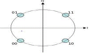
| Quadrature means the signal shifts among phase states that are separated by 90 degrees.The signal shifts as 90 degrees increments from 45° to 135°, - 45° (315°), or -135° (225°) data into the modulator and is separated into two channels
called I and Q.These two bits are transmitted one per channel simultaneously. |
| A better way to represent PSK schemes is using diagram. The points are shown in the complex plane where, in this
regard, the real and imaginary axis are termed as in-phase and quadrature axes respectively due to their 90° separation.
In PSK, the constellation points chosen are positioned with uniform angular spacing to give maximum phaseseparation
between adjacent points around a circle and thus the best immunity to corruption. They are positioned on a
circle to transmit all of them with the same energy. |
3.1 QAM (QUADRATURE AMPLITUDE MODULATION) |
| Quadrature amplitude modulation is both an analog and a digital modulation scheme. It sends two analog message
signals, or two digital bit streams, by modulating the amplitudes of two carrier waves, using the amplitude-shift
keying(ASK) digital modulation scheme or amplitude modulation (AM) analog modulation scheme. The two carrier
waves, that are sinusoids, are out of phase with each other by 90° and hence are called quadrature components —
hence the name of the scheme. The modulated waves are added, and the resulting waveform is a combination of
both phase-shift keying (PSK) and amplitude-shift keying (ASK), or (in the analog case) of phase modulation (PM) and
amplitude modulation. In the digital QAM, a finite number of at least two phases and at least two amplitudes are used.
PSK modulators are usually designed using the QAM principle, but are not considered as QAM since the amplitude of
the modulated carrier signal is constant. QAM is used widely as a modulation scheme for
digital telecommunication systems. Arbitrarily high spectral efficiencies can be achieved with QAM by setting a finite
constellation size, limited only by the noise level and linearity of the communications channel. |
3.2 16-QAM: (16-state quadrature amplitude modulation) |
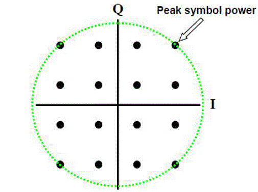
| Four I values and four Q values are used, yielding four bits per symbol 16 states since 24 = 16.Theoretical bandwidth
efficiency is four bits/second/Hz.data is split into two channels, I and Q. As with QPSK, each channel will take on two
phases. However, 16-QAM also accommodates two intermediate amplitude values. Two bits are routed to each channel
simultaneously. The two bits to each channel are added, then applied to the respective channel’s modulator. |
3.3 DESIGN METHODOLOGY OF ADDRESS GENERATOR |
| The deinterleaver address for the first four rows and five columns of each modulation type |
| • Ncbps=no.of code words=96 |
| • J=row numbers=0,1,…….(d-1). |
| • i=column numbers=0,1,……..(Ncbps/d)-1. |
| • Kn=deinterleaver addresses. |
| • No.of rows=d=16(fixed) |
| • No.of columns=Ncbps/d=96/16=6 |
IV. THE PROPOSED ALGORITHM |
| The following algorithm for the QPSK and 16-QAM modulation schemes are proposed. These algorithm are also
tested on MATLAB. Results obtained are verified with the previous MATLAB program for all code rates and
modulation schemes of the WiMAX deinterleaver. |
| A. QPSK |
| Initialize Ncpbs and d For j=0 to d-1, j++ |
| For i=0 to (Ncpbs/d)-1, i++ |
| Kn=d*i + j |
| end for |
| end for |
| B. 16-QAM |
| initialize Ncbps and d |
| for j = 0 to d − 1, j ++ |
| for i = 0 to (Ncbps/d) − 1, i++ |
| if (j mod 2 = 0) |
| kn = d * i + j |
| else |
| if (imod 2 = 0) |
| kn = d * (i + 1) + j |
| else |
| kn = d *(i − 1) + j |
| end if |
| end if |
| end for |
| end for |
V. TRANSFORMATION INTO CIRCUIT |
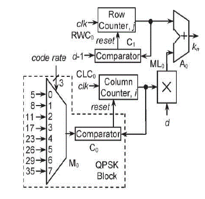
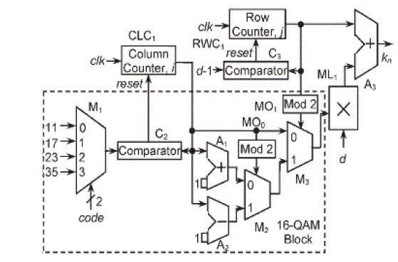
| The address generator of the WiMAX deinterleaver with QPSK and 16-QAM hardware is as shown in Fig 5. The
QPSK hardware has a row counter RWC0 to generate row numbers between 0 and d − 1. A column counter CLC0 with
multiplexer M0 and comparator C0 generate the variable column numbers to implement permissible Ncbps. A multiplier
M0 and an adder A0 perform the desired operations to implement deinterleaver address for QPSK. The address
generator for 16-QAM follows as similar structure, such as that of QPSK with few additional modules. These modules
are designed with an incrementer, a decrementer, two modulo-2 blocks, and two multiplexers, as shown in fig. 5.2. |
| Implementation of the following blocks is done using verilog hardware description language.The design is optimized
in the sense that common logic circuits such as multiplier, adder, rowcounter, and column counter are shared while
generating addresses for any modulation type. |
VI. SIMULATION RESULTS |
| The proposed hardware of the address generator is implemented using HDL Verilog using the Xilinx ISE.
Simulation results are obtained for all permissible modulation types and code rates using ModelSimXE-III.
The simulation results are verified with the output obtained from the MATLAB program. |
VII. CONCLUSION |
| This paper proposes a novel algorithm including proof for address generation circuitry of the WiMAX channel
deinterleaver supporting QPSK and 16-QAM modulation patterns and all possible code rates as per IEEE 802.16e. The
proposed algorithm is converted into an optimized digital hardware circuit. The hardware is implemented on the Xilinx
FPGA using Verilog. Comparison of our proposed work with a conventional LUT-based method and also with a recent
work show significant improvement on resource utilization and operating frequency. |
Tables at a glance |
 |
 |
| Table 1 |
Table 2 |
|
| |
Figures at a glance |
 |
 |
 |
 |
| Figure 1 |
Figure 2 |
Figure 3 |
Figure 4 |
 |
 |
 |
 |
| Figure 1 |
Figure 2 |
Figure 3 |
Figure 4 |
|
| |
References |
- B. Li, Y. Qin, C. P. Low, and C. L. Gwee, "A survey on mobile WiMAX,‖ IEEE Commun. Mag., vol. 45, no. 12, pp. 70–75, Dec. 2007.
- Y. N. Chang and Y. C. Ding, ―”A low-cost dual mode de-interleaver design,‖ in Proc Int. Conf. Consum. Electron, 2007, pp. 1–2.
- B. K. Upadhyaya, I. S. Misra, and S. K. Sanyal, "Novel design of address generator for WiMAX multimode interleaver using FPGA based finitestate machine", in Proc. 13th Int. Conf. Comput. Inf. Technol., Dhaka, Bangladesh, 2010, pp. 153– 158.
- B. K. Upadhyaya and S. K. Sanyal, ―Design of A Novel FSM based Reconfigurable Multimode Interleaver for WLAN Application,‖IEEECommun. Mag, Feb 2011.
- R. Asghar and D. Liu, ―2D realization of WiMAXchannel interleaver for efficient hardware implementation, in Proc. World Acad.Sci. Eng. Technol., Hong Kong, 2009, vol. 51, pp. 25–29.
- A. A. Khater, M. M. Khairy, and S. E.-D.Habib, "Efficient FPGA implementationfor the IEEE 802.16e interleave"r,‖ in Proc.InConf.Microelectron.,Marrakech, Morocco, 2009, pp. 181– 184.
- Local and Metropolitan Networks—Part 16: Air Interface for Fixed Broadband Wireless Access Systems, IEEE Std. 802.16. 2004, 2004.
- M. N. Khan and S. Ghauri, ―TheWiMAX 802.16e physical layer model,‖ in Proc. IET Int. Conf. Wireless, Mobile Multimedia Netw.,Mumbai, India, 2008, pp. 117–120.
- Dhruvakumar, M.C.Chandrashekhar and Dr M.Z.Kurian,-A Low Complexity Address Generator For WiMAXDeinterleaver, inproc.National Conf. Emerging Trends in Electronics and Communication.,Bellur,Karnataka,2014,pp. 366-369.
|