Keywords
|
| Adder, low power, low voltage, voltage boosting. |
INTRODUCTION
|
| Low voltage design may offer a benefit in terms of flexibility in power sources i.e. different battery options. Low voltage does not necessarily imply low power; the power consumed by a gate is proportional to the active current driving the output of the gate. Hence, delay and power consumption are both dependent on the current. Energy or power delay product is not significantly dependent on the current. Energy required to toggle a bit is more dependent on the load and configuration of the gate. Energy Delay Product (EDP) is more dependent on speed than power and will be improved by increasing the current for a specific supply voltage. Optimal supply voltage for CMOS logic in terms of EDP is close to the threshold voltage of nMOS transistor for specific process. Thus current increased, the Energy Delay Product(EDP) also increased and by the way, the speed is also increased. The current level can be increased by using different initialization voltages to the gates. |
| Bootstrapping is an efficient technique for speed enhancement and power reduction. One of the popular ways of reducing the power consumption of a CMOS digital circuit is to scaling down the supply voltage. This is mainly because the switching power consumption of the circuit has a quadratic dependency on supply voltage. In the extreme case, the circuit can be made to be operated in the sub threshold region for maximum energy efficiency. However this approach is limited to be only used in a low-end design, where speed is the secondary concern, because of severe speed degradation due to small switching current and high performance variability due to process, temperature and threshold voltage variations. For medium and high end design, where speed performance and energy efficiency are both important, that much aggressive voltage scaling is not acceptable, and thereby, a near-threshold voltage design is more suitable for achieving relatively high energy efficiency without severe speed degradation. |
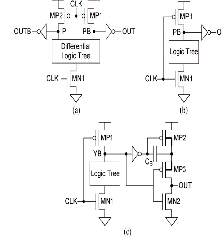
| As the supply voltage scales down toward the threshold voltage, the speed performance of conventional CMOS circuits, such as the static CMOS logic, the differential cascade voltage switch (DCVS) logic [see Fig. 1(a)], and the domino CMOS logic [see Fig. 1(b)], is still severely degraded due to the reduced overdrive voltage (VGS − VTH) of transistors. To overcome this problem, a bootstrapped CMOS large capacitive-load driver was proposed. It was a solution to the speed degradation problem. It can improve the switching speed at low supply voltage by allowing the voltage of some internal nodes to be boosted beyond the supply rails. And here two capacitors are used for bootstrapping purpose. One capacitor for pull up bootstrap circuit and another for pull down bootstrap circuits. However, since the circuit was proposed for use as a large capacitive-load driver, logic functions cannot be efficiently embedded into the circuit and the speed advantage was not fully exploited. And there is an inefficiency in terms of boosted voltage generation due to the driver uses only one bootstrap capacitors for each bootstrapping operation despite having dual bootstrap capacitors in the circuit. |
| For fast logic operation at low supply voltage, CMOS bootstrapped dynamic logic (BDL) [see Fig. 1(c)] was proposed. However, the speed of this logic style was not so much improved since the latency of bulky bootstrapping circuit was superimposed on the overall latency of the circuit. And moreover, logic composition of this logic style is constrained since it is configured as a single ended structure. Although some recent circuit techniques adopting bootstrapped operation have been proposed, they are all not for logic composition but for large capacitance driving. And all proposed ones requires larger area. To overcome the aforementioned problems and to further improve the switching performance, a novel boosting CMOS differential logic style is proposed in this paper. It also minimizes the area and also eliminates the problem of inefficiency. As compared to existing bootstrapped logic, here the advantage of speed is fully exploited. And the latency problem can be solved by giving the voltage boosting block directly to the differential logic tree. |
| Section II describes the circuit structure and operation of the proposed logic style. In Section III, comparison results for some representative logic gates are presented to assess the performance of the proposed logic style. In section IV, describes the experimental result for 64-bit adders as a design example to prove the practicality of the proposed logic style. And finally, present the conclusion in Section V. |
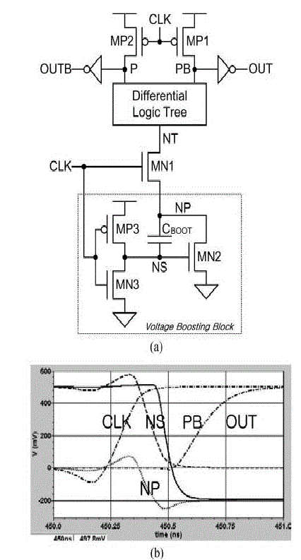
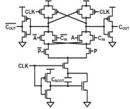
| Fig.2(a) shows a generic structure of the proposed logic style, i.e., boosted CMOS differential logic (BCDL). BCDL consists of a precharged differential logic block and a voltage-boosting block. The voltage-boosting block, which is shown in the dotted box at the bottom part of the circuit, is composed of transistors MN2, MN3, and MP3 and boosting capacitor CBOOT which is used to boost the voltage of NP below the ground. |
| The precharged differential logic block, which is composed of a differential logic tree with bottom transistor MN1, precharge transistors MP1 and MP2, and output inverters which receives the boosted voltage at NP and swiftly evaluates the output logic values. Let us explain the operation of BCDL. BCDL has two phases of operation, namely, a precharge phase and a boosted evaluation phase. When the CLK is low the circuit is in the precharge phase. During this phase, the precharged differential logic block is separated from the voltage-boosting block since MN1 is fully off. Precharge nodes P and PB in the differential logic block are then precharged to the supply voltage by MP1 and MP2, letting outputs OUT and OUTB identically low. At the same time, transistors MP3 and MN2 in the voltage-boosting block turn on, allowing NS and NP to be high and low, respectively. Then, a voltage identical to the supply voltage is applied across CBOOT. When CLK changes to high, the circuit goes into the boosted evaluation phase. |
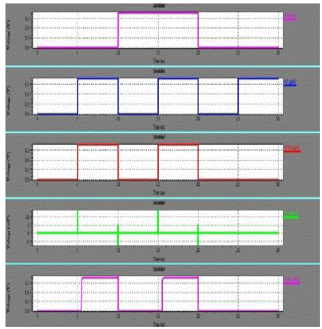
| The simulated waveforms of BCDL in this phase are shown in Fig. 2(b), where a 0.5V supply voltage is used. Since CLK goes high, MN1 turns on and connects the differential logic tree to the voltage-boosting block. At the same time, NS is pulled down toward the ground, and by capacitive coupling through CBOOT, allowing NP and NT to be boosted below the ground. As shown in Fig. 2(b), NP temporally reaches −250 mV and settles at around −200 mV by the boosting action. Then, the gate–source voltages of MN1 and transistors that are on in the logic tree are enlarged this resulting in an increased driving strength of these transistors. And moreover, a slightly forward source–body voltage established in these transistors by boosting source voltages below the ground leads to a reduction in threshold voltages of these transistors, further increasing their driving strength. In turn, the boosted voltage at NT is then transferred to P or PB through the logic tree, depending on input data. [In Fig. 2(b), input data are such that PB is pulled down below the ground]. The gate–source voltage of the driver pMOS transistor is also enlarged and this enhances its driving strength. Along the timing-critical signal paths from the inputs to the outputs via precharge nodes all these driving strength-enhancing effects by boosting are combined together, resulting in significantly improved switching speed at a low-voltage region. |
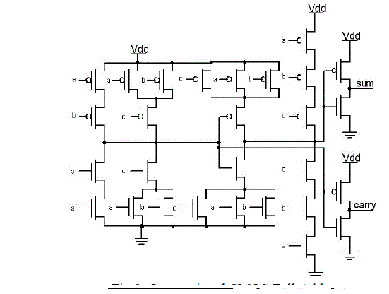
| Figure.3 shows the conventional CMOS 28-transistor adder. I am using this circuit for Differential logic tree and logic tree block for Fig. 1(a) and Fig. 1(b). The CMOS structure combines PMOS pull-up and NMOS pull-down networks to produce considered outputs. In this style all transistors (either PMOS or NMOS) are arranged in completely separate branches and each may consist of several sub-branches. The mutually exclusiveness of pull-up and pull-down networks is of a great concern. One possible implementation of the full adder is the Mirror Full Adder. The mirror full adder circuit device consists of 28 total transistors (4 transistors used for the construction of two inverters). Hence the full adder acts as a fundamental building-block component to larger circuits units, timing and power consumption optimization efforts at the adder level can lead to improved circuit throughput ratings, enhanced speed performance, and lowered power consumption requirements. Therefore, at this fundamental level it is very important to minimize latency and resolve any timing issues in order to avoid issues inevitably brought about by scaling. |
III. SIMULATION COMPARISON
|
| To assess the performance of the proposed circuit technique, various multi-input logic gates are designed using the conventional and proposed logic styles in a tsmc0.18-μm CMOS process. The nominal threshold voltages of p- and nchannel MOS transistors are −0.45 and 0.42 V, respectively. The boosting capacitor was implemented using the gate-oxide capacitance of a pMOS transistor. Transistor widths in each logic gate and the amount of boosting capacitance were individually optimized at each supply voltage for each logic style to provide a minimum energy–delay product (EDP). |
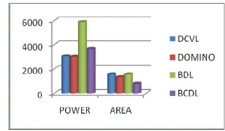
| The table I summarizes the simulated performance of various logic gates designed with the conventional and proposed logic styles. The simulation was executed at 100-MHz frequency with a supply of 1.8V. In the domino CMOS and BDL, only the non-inverting outputs are available. For Full adder which having the same input counts designed with differential logic styles, the BCDL gates has larger energy as compared with domino CMOS and DCVS gates due to the extra circuit to perform the boosting operation, it consumes still less energy than BDL gates. In case of EDP, BCDL gates show the best performance, improvement over the conventional logic gates. The fig.4 shows the power analysis in different types of circuits such as DCVL, DOMINO, BDL, BCDL. |
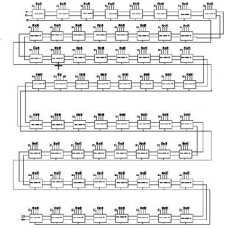
| To demonstrate practical applicability of the proposed logic style, a set of 64-bit adders were designed. The 64-bit adder consisting of eight 8-bit adder subsections adopts the carry selection scheme for high-speed carry propagation. In BCDL Adder an 8-bit ripple carry chain was used to allow boosting operation at each carry chain stage, whereas an 8-bit Manchester carry chain was used in the DCVS and BDL adders for high-speed carry propagation. Fig. 6 shows the structure of the 8-bit ripple carry chain used in the 64-bit BCDL adder. |
| At 0.5-V supply voltage, the 8-bit carry chain in the BCDL adder requires 2.14 ns for propagating a carry value from the lowest to the highest bit positions, whereas the 8-bit carry chains in the DCVS and BDL adders require 8.96 and 7.48 ns, respectively, indicating 76% and 72% improvements. In 8 bit ripple carry adder chain the average power consumed is 259.5673 milli watts. |
| The power, EDP, and PDP levels all are reduced compared to Exciting methods of DCVL, DOMINO CMOS, BDL. In BCDL, the outgoing carry from each 8-bit subsection goes into block-carry generators (BCG). There is a pair of BCGs in each 8-bit subsection in the upper half of the adder, and block carries are selected using the carry bit propagated from the lower half. The measured propagation delay and switching energy of the BCDL adder depending on supply voltage are summarized in table II. |
V. CONCLUSION
|
| CMOS differential logic style with voltage boosting has been described. The BCDL provides higher switching speed than the conventional logic style at low supply voltage. By allowing a single boosting circuit to be shared by complementary outputs the BCDL minimizes the area overhead. Comparison results in a 0.180-μm CMOS process indicated that the energy–delay product of the proposed logic style was improved when compared with conventional logic styles. Here present two high-speed and low-power full-adder cells designed. Logic styles that lead to have a reduced power-delay product (PDP). The experiment result for a adder designed with BCDL logic style revealed an reduction in the addition time. |
Tables at a glance
|
 |
 |
| Table 1 |
Table 2 |
|
| |
Figures at a glance
|
 |
 |
 |
 |
| Figure 1 |
Figure 2 |
Figure 3 |
Figure 4 |
 |
 |
 |
| Figure 5 |
Figure 6 |
Figure 7 |
|
| |
References
|
- Jong-Woo Kim, Joo-Seong Kim, and Bai-Sun Kong, “Low-Voltage CMOS Differential Logic Style With Supply Voltage Approaching Device Threshold” IEEE transactions on circuits and systems—ii: express briefs, vol. 59, no.3, march 2012
- Wang A and Chandrakasan A, “A 180 mV FFT processor using subthreshold circuit techniques,” in Proc. IEEE ISSCC, 2004, pp. 292–295.
- Zhai B, Nazhandali L, Olson. J, Reeves A, Minuth M, Helfand R, Sanjay P, Blaauw D, and Austin T, “A 2.60 pJ/Inst subthreshold sensor processor for optimal energy efficiency,” in Proc. IEEE VLSI Symp., 2006, pp. 154–155.
- Garcia J, Montiel-Nelson J A, and Nooshabadi S, “A single-capacitor bootstrapped power-efficient CMOS driver,” IEEE Trans. Circuits Syst. II, Exp. Briefs, vol. 53, no. 9, pp. 877–881, Sep. 2006.
- Kim J W and Kong B S, “Low-voltage bootstrapped CMOS drivers with efficient conditional bootstrapping,” IEEE Trans. Circuits Syst. II, Exp. Briefs,vol. 55, no. 6, pp. 556–560, Jun. 2008.
- Lou J H and Kuo J B,, “A 1.5-V CMOS all-N-logic true-single-phase bootstrapped dynamic-logic circuit suitable for low supply voltage and high-speed pipelined system operation,” IEEE Trans. Circuits Syst. II, Analog Digit. Signal Process, vol. 46, no. 5, pp. 628–631, May 1999.
|