International Journal of Advanced Research in Electrical, Electronics and Instrumentation Engineering
ISSN ONLINE(2278-8875) PRINT (2320-3765)
ISSN ONLINE(2278-8875) PRINT (2320-3765)
T.S.Ghouse Basha1 and S.Emmanuel Steeven Singh2
|
| Related article at Pubmed, Scholar Google |
Visit for more related articles at International Journal of Advanced Research in Electrical, Electronics and Instrumentation Engineering
Multiplier is one of the key hardware blocks in most digital and high performance systems such as FIR Filters, Digital Signal Processors, and Multiprocessors. In the proposed work, the Multiple Constant Multiplication / Accumulation (MCMA) block of FIR filter is implemented using Xilinx 14.1 Simulator. High speed multiplication is performed using Column Compression Multipliers such as Wallace and Dadda Multipliers. The Column Compression multipliers divide the Partial Product Summation Tree (PPST) into two parts so that the column compression can be achieved in parallel independently and reduces to a height of 2 bit column finally. The Hybrid Final Adder uses Multiplexer Binary Excess Converters (MBEC) which further accelerates the speed and consumes less area
Keywords |
| MCMA Block, Column Compression Multipliers, MBEC, Hybrid Final Adder |
INTRODUCTION |
| Finite Impulse Response (FIR) filter is one of the primary used digital filter in Digital Signal Processing (DSP) and communication systems. As it can be easily designed to linear phase and implemented easily by simple looping and can support multi-rate applications by consuming less area and power it is widely used in portable applications. For implementing the FIR filter we need multiplier, adder, delay & storage modules. Multiplier block has huge impact on complexity & performance of system as it requires huge no of Multiple Constant Multiplication / Accumulation. |
| The two most commonly used structures of FIR filters are direct structure and transposed structure shown in Fig. 1 |
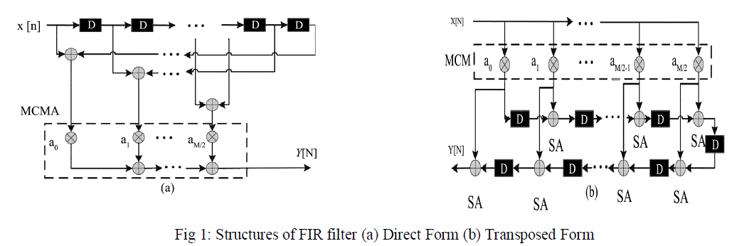 |
| As shown in Fig 1(a) the delayed input signal x[n-i] is multiplied with the appropriate filter coefficient ai and the products are accumulated after multiplication process in the Direct Form whereas the input signal x[n] is multiplied with the appropriate filter coefficient and the result of each constant multiplication go through the Structural Adders (SA) and delay elements in the transposed form shown in Fig 1(b). |
LITERATURE SURVEY |
| The complexity of digital filter is greatly influenced by the no of multiplication needed in the multiplier block. The complexity can be greatly reduced if efficient number system is used.[2] proposed an efficient MSD representation which can provide no of forms which has minimum no of nonzero digits for the constant. |
| The multiplier block of digital FIR filter has significant impact on the complexity and performance of the design because large numbers of constant multiplications are required to achieve high through-put and the multiplication operation is considered to be expensive as it occupies significant area. [3] Proposed efficient shift-add design of digitserial multiplications and yielded significant area and power reduction than those compared with the multiplier blocks which are implemented by using digit –serial constant multiplier. Hence the multiplications of input data with filter coefficients is done using shift-add architectures where each constant multiplication is realized by using addition/subtraction and shift operation in Multiple Constant Multiplication(MCM) block. |
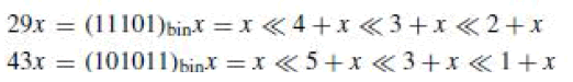
| The easiest method for implementing shift-add architecture is digit-based-recording method. In this method we first define the constant in the binary and for each “1” in the binary representation of constant , according to the bit position it shifts the variable and adds up to the shifted variable in order to obtain the desired result. For example we will see the representation of 29 and 43. |
 |
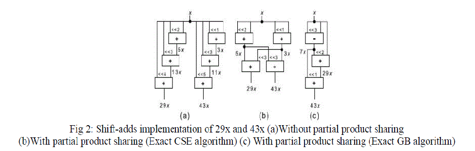
| The disadvantage of this method is that it does not exploit the sharing of the partial products(PP) which greatly reduces the number of operations required which in turn decreases the area and power dissipation of MCM design at gate level. It is clear from the representation of the constants 29 and 43 requires 6 addition operations as shown in the fig 2. So there is need to optimize the number of addition/subtraction operations for constant multiplication. |
 |
| Many applications in DSP, telecommunications, graphics, require large no of multiplications of one variable with several constants. So optimization in Multiple Constant multiplication will lead to significant reduction in power, area and increases the throughput. [4] Proposed a formula for MCM problem to solve it where minimum numbers of shifts are computed first and then attention is paid to reduce the no of addition operations using common sub expression elimination which is based on iterative pair wise matching |
| Multiplier block is critical in designing FIR filter since it consumes more power. In designing the Multiple Constant Multiplication (MCM) [5] proposed a novel common sub expression elimination (CSE) algorithm that represents synthesis of coefficients into cost function. Though the algorithm could not find the optimal solution, it is capable of providing minima of the function and discovered relationship between MSD representation and shifted sum of coefficients. |
| In-Cheol Park and Hyeong-Ju Kang et al [6] proposed an algorithm to find all possible minimal signed digit (MSD) representations for a constant. He presented an algorithm to synthesize digital filters based on the MSD representation. Based on the number system that is used for the implementation the hardware complexity of DSP system will vary. Inspite canonical signed digit (CSD) produces minimal number of nonzero digits for a constant; the MSD representation provides several representations that have the same number of nonzero digits as the CSD representation. The proposed filter synthesis algorithm utilizes this redundancy of the MSD representation to make multiplier size small in filters. By applying the proposed algorithm to the hardware synthesis of finite impulse response filters, the authors obtained multiplier blocks that are 7% smaller than those generated from the CSD representation. |
| The final carry propagate Adder inside the multiplier place an important role in determining the performance of multiplication block.[12] presented an algorithm to generate the optimal width configuration for each of the sub-adders. This technique is very useful in choosing the best configuration of hybrid adder which improves the performance. |
| In VLSI system design it is required to design system which consumes low area and power and simultaneously has high speed data path logics. In digital adders, the speed of addition is restricted by the time required to propagate a carry through the adder. The sum of each bit position in an elementary adder is generated sequentially only when the previous bit position has been summed and a carry propagated into the next successive position. [14] suggested that use of BEC instead of RCA to decrease the area and power requirements as BEC needs few logic gates when compared with the Full Adder Structure.In this paper, we are using MBEC in the final adder design to still decrease the area and power requirements. |
DESIGN OF FIR FILTER |
| Generally for designing the FIR filter, the following five stages are required |
| A. Filter specification: Initially we need to specify the type of filter (low pass filter,high pass filter etc.,) the amplitude and/or phase responses and the tolerances required in order to get the desired response, the sampling frequency, the word length of the input data and order of the filter. Parks Mc_Clellan method is mostly used to find the order of the filter |
| B. Filter coefficient calculation: In this stage, calculation of the coefficients of a transfer function H (z) that satisfies the given specification is determined. The most commonly used methods for calculating the filter coefficients are window method, frequency sampling method and the optimal methods. Mostly the MATLAB built-in function remez() is used to find the coefficients for the given specification. |
| C. Choosing the structure of filter: The two mostly used FIR structures are transposed method and direct method. In this stage the transfer function is converted to the suitable structure according to specification. |
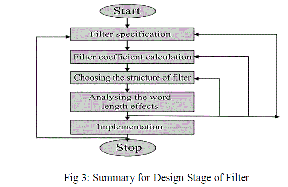 |
| D. Analysing the word length effects: In this stage the coefficients of the filter are quantized initially and the frequency response of the quantized coefficients is checked with the help of sub-routine freq_resp_satisfied() and if the routine yields the positive results then the quantized coefficients are taken or else they remain the same. Then recoding is performed using either CSD recoding which uses {0, 1, -1 } or radix-4 modified Booth recoding which uses {0,1,- 1,2,-2} to minimize the number of non-zero digits in order to achieve the smaller area cost. After that non-uniform quantization is performed on the coefficients to reduce the bit-width of the coefficients. The reduction continues till the frequency response is satisfied. |
| E. Implementation: In the final stage implementation of the filter is performed using software and/or hardware.In the proposed work, high speed implementation of multiplications of the MCMA module in direct structure of FIR filter using column compression multipliers for reduction of partial product is presented. The bit width of all the filter coefficients are reduced using non-uniform quantization of unequal word lengths in order to decrease the cost of hardware and simultaneously achieving the desired frequency response. We adopted the direct form structure of MCMA module because it offers less area cost of flip-flops in the delay elements when compared with the transposed form. |
| In MCMA module, the bit width of output signals increases due to expansion of bits after multiplication. But in pratical we require only partial bits of full precision output signals. For example if the input signal of the FIR filter consists of 12 bits and the coefficients are quantized to 10 bits, the bit width of the output signal contains minimum of 22 bits. But we need only 12 bits for further processing. Therefore we require multipliers which can faithfully round the resultant output signals to the required bit length still meeting the performance requirements.In this proposed work we are implementing the multiplier module. |
MULTIPLICATION SCHEMES |
| Multiplier is one of the fundamental blocks in most digital and high performance systems like FIR filters, digital signal processors, multiprocessors etc., The performance of the system greatly depend on the performance of the multiplier. Therefore it is needed to design the multiplier which consumes less area and power which guarantees correct results at high speed. To enhance the speed the digital multipliers are generally implemented in hardware which generates all bit products and add them in parallel using an array or tree of adding elements. In recent days column compression multipliers have gained the popularity due to their high computation speeds. The two well known fast multipliers are |
| • Dadda Multiplier |
| • Wallace-Tree Multiplier |
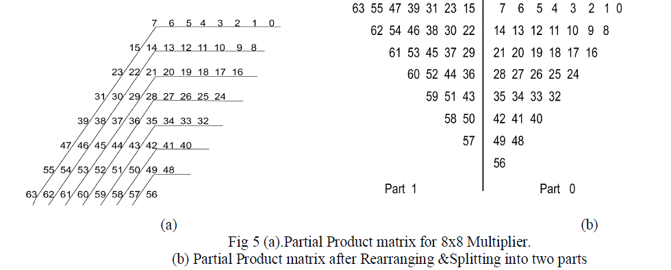
| Both the schemes require three processes, namely formation of product bit matrix, reduction of product bit matrix to two row matrix, summation of the final two rows using appropriate adder. In Wallace method, the partial products are reduced immediately after their formation whereas in Dadda method it performs the minimum reduction that is required at each level and reduce in the same number of levels that are required by the Wallace method. |
A. Wallace Multipliers |
| In Wallace multipliers, the partial product matrix is formed with the help of N2 AND gates in the same procedure in the DADDA multiplier. In the next level, N rows are grouped into the sets of 3 each and (3, 2) counters are applied and sets of 2 each for the columns containing only 2 bits and (2,2) counters are applied and the column containing only single bit are transferred to next level unchanged.The height of matrix in the jth reduction stage is given by the following recursive equations |
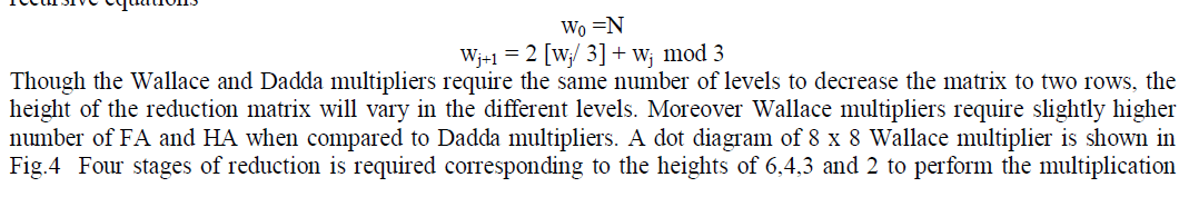 |
| process. In the fig two dots joined by the diagnol line represent the output of the (3,2) counter and the two dots joined by the crossed diagnol indicate the output from the (2,2) counter. It requires total of 64 AND gates, 1 OR gate ,38 (3,2) counters and 15 ( 2,2) counters and 10 bit CLA to form 16 bit product whereas the Dadda multiplier requires 64 AND gates, 35 (3,2) counters ,7 (2,2) counters and 14 –bit carry propagate adder. |
 |
| The no of (3,2) counters required by the Wallace multiplier depends on the bit width and number of stages in the reduction and the no of (2,2) counters will be greater than or equal to N and in most cases it requires greater than N which results in more area despite of smaller carry propagating adder |
 |
 |
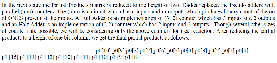 |
| The final row of part 0 part 1 and are added using a Carry Look-ahead Adder (CLA) to form the final partial products which has only a height of one bit column. In Part 0 the bits from 8 to 10 (p0 [10:8]) are the exceeding carry bits of part0 and final bit of Part 1 via p1 [15] is the carry bit of part1.. To find remaining p [15:8], we use the CLA and the MBEC shown in Fig. 6. |
THE HYBRID FINAL ADDER DESIGN |
| In existing system the hybrid final adder designs use CLA (Carry Lookahead Adder) and CSLA (Carry Select Adder) in order to achieve the faster performance in parallel multipliers. But structure of the CSLA,requires more chip area than other adders. Thus to achieve the optimal performance, the proposed hybrid adder in this work uses MBEC (Multiplexers with Binary to Excess-1 Converters) and Ripple Carry Adder (CLA) which can successfully take care of uneven input arrival time of the signals originating from the PPST and perform addition very fast. The MBEC adder provides faster performance than Carry Save Adder (CSA) and Carry Look Ahead (CLA) adder. Also it consumes less area and power than the Carry Select Adder (CSLA). |
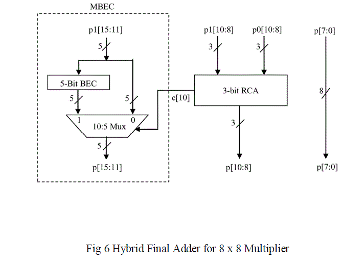 |
| The first seven bits p[7:0] of part0 are directly assigned as the final products .The excess bits of part 0 via p0[10:8] and the three LSB’s of Part 1 via p1[10:8] are added using 3-bit CLA which finds p[10:8]. To obtain the remaining p[15:11], the p1[15:11] are assigned to the input of 5-bit MBEC, which produce the two partial results p1[15:11] with Carry (Cin) of ‘0’ and the 5-bit BEC output with the Carry (Cin) of ’1’. Depending on the Carry of the MSB bit ( Cout) of CLA(c[10]), the mux provides the final p[15:11] without having to ripple the carry through p1[15:11]. |
| The 8-bit multiplier uses a single 5-bit MBEC in the final adder. But the large bit sized multipliers requires multiple MBEC and each of them requires the selection input from the carry output of the preceding MBEC. Therefore to generate the carry output from the MBEC, an additional block is developed which is called MBECWC (MBEC With Carry). The detailed structures of the 5-bit BEC without carry (BEC) and with carry (BECWC) are shown Fig. 7(a) and Fig. 7(b). The BEC gets n inputs and generates n output; the BECWC gets n input and generates n+1 output to give the carry output as the selection input of the next stage mux used in the final adder design of 16, 32 and 64-bit multipliers. |
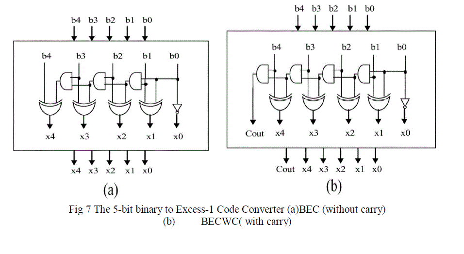 |
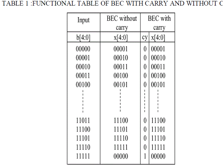
| The function table of BEC and BECWC are shown in Table 1. |
 |
EXPERIMENTAL RESULTS |
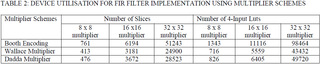
| Device Utilisation for 3 frequently used multiplier schemes for the implementation of 8 bit,16 bit and 32 bit are shown in the Table 2 The results shows that the Wallace multiplier occupies less area of all in the multiplier schemes. |
 |
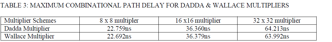
| The maximum combinational path delay for the two column compression multipliers are tabulated in Table 3.The results shows that we can achieve the output results in nanoseconds itself using the proposed algorithm. |
 |
CONCLUSION |
| This brief has presented low-cost FIR filter designs by jointly considering the optimization of coefficient bit width and hardware resources in implementations. Although most prior designs are based on the transposed form, we observe that the direct FIR structure using column reduction multipliers with the hybrid adder results in fast results of FIR simultaneously reducing the area cost as the direct structure needs less number of flipflops than transposed structure. |
References |
|