International Journal of Advanced Research in Electrical, Electronics and Instrumentation Engineering
ISSN ONLINE(2278-8875) PRINT (2320-3765)
ISSN ONLINE(2278-8875) PRINT (2320-3765)
| A.Lakshminarayanan and S.Ganesan Assistant Professor, Dept. of ECE, Kongunadu College of Engineering and Technology,Thottiam, Tamilnadu, India |
| Related article at Pubmed, Scholar Google |
Visit for more related articles at International Journal of Advanced Research in Electrical, Electronics and Instrumentation Engineering
In this paper a fully synchronous circuit for embedded DRAMs is presented. It realizes accurate DRAM timing control, and easy timing adjustment, power dissipation analysis for 3T DRAM cell and 4T DRAM cell design have been carried out for the Nanoscale technology. Many advanced processors now have on chip instructions and data memory using DRAMs. The major contribution of power dissipation in DRAM cell is off-state leakage current. Thus, improving the power efficiency of a DRAM cell is critical to the overall system power dissipation. This paper investigates the effectiveness of 3T DRAM cell and 4T DRAM cell circuit design techniques and power dissipation analysis. 3T DRAM cell is designed with the semantic design technique for the analysis of power dissipation using CADENCE Tool. In this paper, we have taken two circuits of dynamic random access memory (DRAM). Read and write operation for single bit storage of 3T DRAM and 4T DRAM circuit is shown by simulating it on Tanner EDA tool.
Keywords |
| DRAM, Power dissipation, Timing control, Leakage current |
INTRODUCTION |
| Since the address multiplex scheme was adopted into the 4K-bit MOS DRAM, conventional DRAMs have kept their asynchronous design for over 20 years. Careful timing control is necessary to sense a small voltage signal of the 1Tr/1C memory cell. To fine-tune the timing, the internal DRAM control signals are generated as the delay signals of the Row Address Strobe signal(/RAS) or the Column Strobe signal(/CAS), with series of delay elements. |
| The DRAM operation isn't synchronized with a system clock because enough internal clock edges could not be produced with the system clock. Recently, several high speed DRAMs have been introduced [1-3]. All of them operate synchronously with the system clock, but only I/O circuits and address paths are replaced with the synchronous circuits. Basically, most of their internal control circuits remain asynchronous. This is also true in the previous CPU embedded DRAM. The demerits of the asynchronous control with the delay elements are follows: |
| (1) Access time is considerably affected by the supply voltage and temperature. |
| (2) The actual waveforms are usually different from the simulated results due to the large dependency of the Process parameter. |
| (3) Large area is occupied with the additional delay elements to fine-tune the timing. |
| A. FIRST STEP: ROW ADDRESSES |
| Row addresses are present on address pads and are internally validated by the RAS (Row Address Access) clock. A bar on top of the signal name means this signal is active when it is at a low level. The X addresses select one row through the row decode, while all the other non-selected rows remain at 0V. Each cell of the selected row is tied to a sense amplifier. Sense amplifier is a circuit that is able to recognize if a charge has been loaded into the capacitor of the memory cell, and to translate this charge or lack of charge into a 1 or 0. There are as many sense amplifiers as there are cells on a row [3]. Each sense amplifier is connected to a column (Address). In this first step all the cells of the entire row are read by the sense amplifier. This step is long and critical because the row has a high time constant due to the fact that it is formed by the gates of the memory cells. Also, the sense amplifier has to read a very weak charge (approximately 30 femtoFarads or 30fF). |
| B. SECOND STEP: COLUMN ADDRESSES |
| Following the first step, column addresses are present on the address pads and are internally validated by the Column Address Access (CAS) clock. Each selected memory cell has its data validated in a sense amplifier. Column access is fast. This step consists of transferring data present in the sense amplifier to the Dout pin through the column decode and the output buffer [4]. On memory data sheets, the access time from RAS is termed tRAC and the access time from CAS is listed as tCAC. On a typical standard DRAM of 60ns access time, tRAC = 60ns and tCAC = 15ns. |
| C. REFRESH CYCLE |
| To maintain data integrity, it is necessary to refresh each DRAM memory cell. Each row of cells is refreshed every cycle. For example, if the product specification states, “Refresh cycle = 512 cycles per 8ms,” then there are 512 rows and each individual row must be refreshed every eight milliseconds. As explained above, during the row access step, all the cells from the same row are read by the sense amplifier. The sense amplifier has two roles. Since it holds information within the cell, it is able to transmit this data to the output buffer if it is selected by the column address. The sense amplifier is also able to re-transmit (write) the information into the memory cell. In this case, it “refreshes” the memory cell. When one row is selected, all the cells of that row are read by the sense amplifiers and all these cells are refreshed one at a time. |
LITERATURE REVIEW OF DIFFERENT DRAM CELLS |
| Technical requirements for DRAMs have become more difficult with scaling [5]. As an example lithography to define smaller dimensions is becoming increasingly more difficult. The process associated with 193 nm argon fluoride (ArF) immersion high-numerical aperture lithography and double patterning technology are keys for 40 nm or smaller half-pitch DRAMs. In recent years, DRAM cell structure has been migrating to stack capacitor cell. Trench DRAM cell could not survive future scaling due to its difficulties of getting the adequate process and performance of the memory cell. But, even the stack capacitor cell has many technology challenges for 40 nm or smaller size DRAM. |
| However, there exist several significant process flow issues from a production standpoint, such as process steps of capacitor formation or high aspect ratio contact etches requiring photo resist that can stand up for a prolonged etch time. To overcome these challenges, the technology related to photo resist with a hard mask layer for pattern transfer is gaining importance. Furthermore, continuous improvements in lithography and etch will be needed [7]. On the other hand, with the scaling of peripheral CMOS devices, a low temperature process flow is required for process steps after formation of these devices. This is a challenge for DRAM cell processes which are typically done after the CMOS devices are formed, and therefore are limited to low-temperature processing. |
| In addition, the planar access device (cell field-effect-transistor (FET)) for the one transistor-one capacitor (1T/1C) cell is becoming difficult to design due to the need to maintain a low level of both subthreshold leakage and junction leakage current to meet the retention time requirements. To attain that, recessed channel cell FET is being adapted and optimization work have been done under half-pitch scaling. But below the 40’s nm half-pitch, FinFET or 3-D type FET will be required to get the high drive current and low-voltage operation. Another challenge is a highly reliable gate insulator. A highly boosted gate voltage is required to obtain higher drain current with the relatively high threshold voltage adopted for the cell FET to suppress the sub threshold leakage current [8]. |
PROPOSED SYNCHRONOUS DRAM ARCHITECTURE BASICS |
| This paper proposes a fully synchronous control circuit for embedded DRAM. The merits of the fully synchronous Circuit are as follows: |
| (1) The control timing is accurate, because it is generated by counting the number of the external clocks. |
| (2) Typical ASIC standard cells can be used for the DRAM control logic. |
| (3) The circuit is suitable to employ logic synthesis and Place & Router tools. |
| In addition to these merits, the following functions can be easily implemented in the CPU embedded DRAM. |
| • Software switching of the DRAM control timing is realized with no difficulty. |
| • Providing handshake signals to on-chip memory-controller simplify the controller circuit in a CPU embedded DRAM. |
DRAM CONTROL SIGNALS & TIMING |
| The typical address and data paths of the DRAM are shown in fig.1; the DRAM read-operation is destructive, careful timing control of the row operation is necessary as described below: |
| (1) The row address decoding can't be started until after the addresses are latched to prevent temporary and unexpected word-line selection. |
| (2) The word line should not be activated until the equalization signal of the bit line is completely deactivated. |
| (3) The bit line should be sensed after the memory cell data is sufficiently transferred to it. |
| For the column control, careful control is necessary for the points listed below: |
| (1) The CDE signal should not be activated until after the column addresses are latched to prevent the invalid data from being transferred to the I/O line. |
| (2) The PAE signal should be asserted after the bit line data is sufficiently transferred to the I/O line. |
BLOCK DIAGRAM OF THE FULLY SYNCHRONOUS CIRCUIT |
| The block diagram of the fully synchronous DRAM control circuit is shown in fig.2. The circuit consists of the row and column counters, and the control signals generator. Each counter operates synchronously with the positive edges of both clock P1 and clock P2, which are non-overlapped complementary clocks. The row counters are controlled with the Row-Activation-Request (ACT) signal and the Row-Precharge-Request (PCG) signal. The column counter is controlled by the Read-Operation-Request (RREQ) signal and Write-Operation-Request (WREQ) signal. Each request signal is generated by the memory controller, synchronized with clock P2, and sampled at the edge of clock P1. The DRAM control signal generator uses the row and column outputs to create its outputs. |
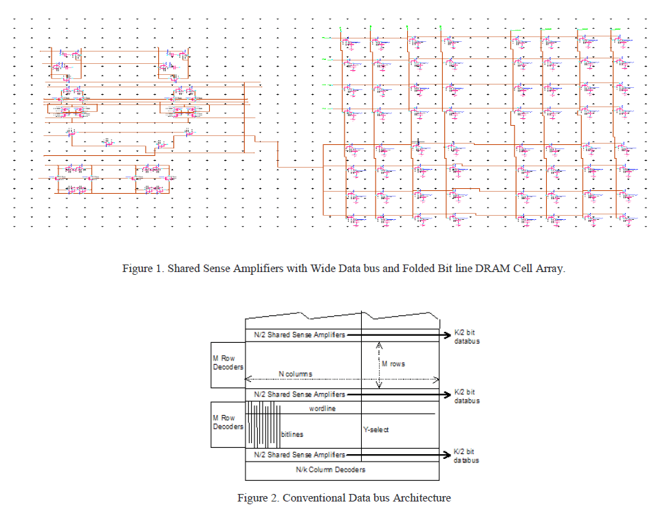
| Figure 3 shows the core circuitry of a DRAM, including cells, sense amplifier, and data path. In the folded bit line architecture a word line connects a memory cell to either BL or BL* in each column of the array. The other bit line acts as a reference during sensing. Word lines WL are driven to Vpp, a voltage supply higher than Vdd, to allow a full Vdd level to be written to the cell capacitor through the n-channel access transistor. Here, the sense amplifier is shared between top and bottom arrays, as selected by an isolation signal ISO which is also driven to a Vpp level. Prior to sensing, the bit lines and sense amplifiers are precharged to Vdd/2 by the equalization signals EQ. At the beginning of an active row cycle, the appropriate EQ signals are de-asserted and a single word line is raised to Vpp sharing the charge in the cell capacitor with the bit line capacitance. The bit line to cell capacitance ratio is typically 5:1, so the cell signal is attenuated significantly. Sense amplifiers are then activated by simultaneously ramping sense clocks PR and PS* from the Vdd/2 precharge state to Vdd and Vss respectively, to power the cross coupled latch. Depending on the polarity of the data, one of the bit lines will swing to Vdd and the other to Vss. This restores the full data to the memory cell. In Figure 1 a differential bidirectional databus DB/DB* is shared by two columns of sense amplifiers. |
| Typical commodity DRAM data busses run parallel to the word lines through the sense amplifier area as shown in Figure 3. Multiple arrays are activated and a small number of bits are provided by each array. This provides sufficient data to feed the limited I/O bandwidth of a standalone memory chip. |
 |
SIMULATION RESULTS AND DISCUSSION |
| All the circuits have been simulated using BSIM 3V3 90 nm and 45nm technology on Tanner EDA tool with supply voltage ranging. |
 |
 |
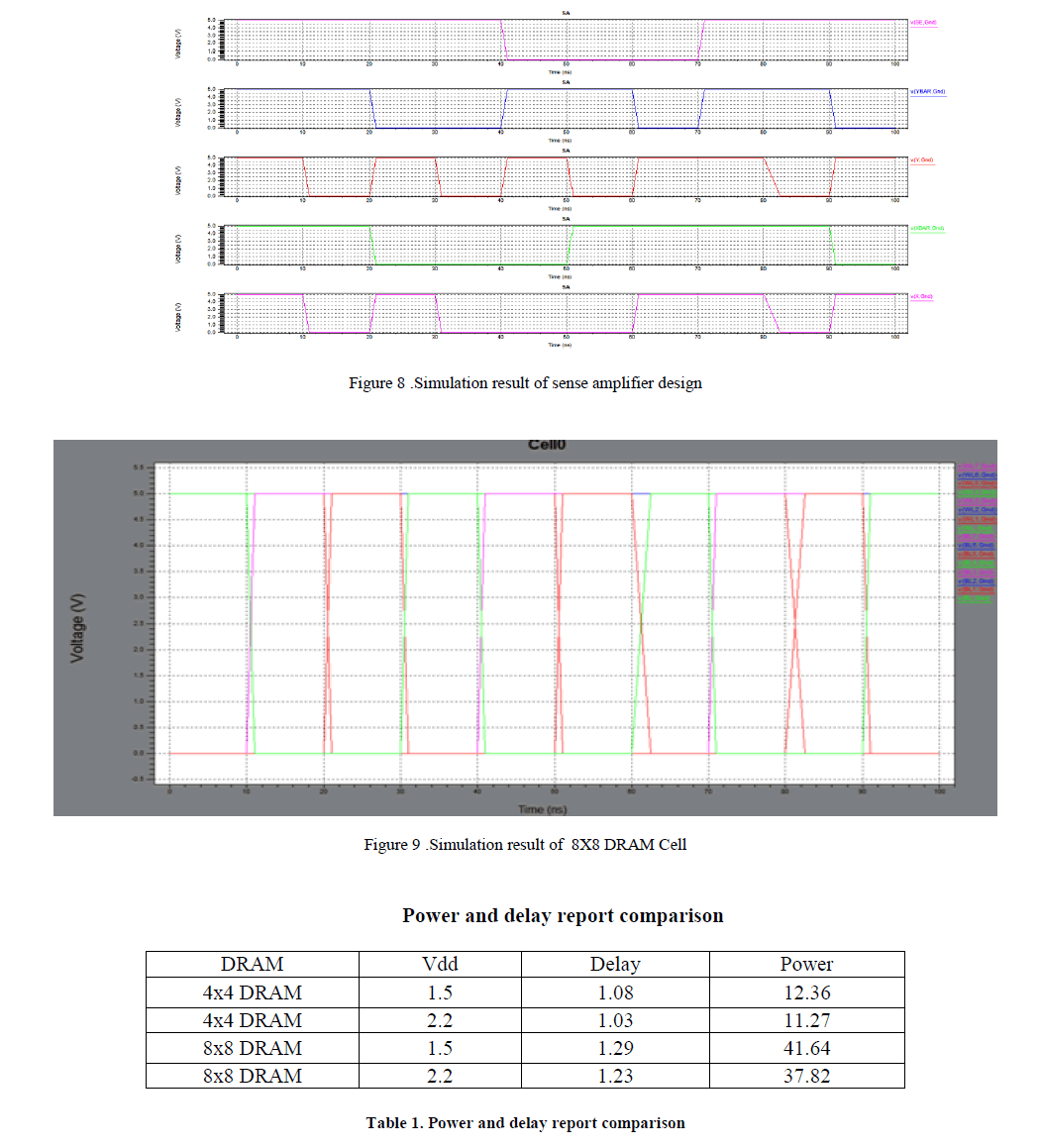
| The waveforms which were generated with the fully synchronous circuits from fig.4 are shown in fig.5. The enable period of each control signal depends on the counter value. Because there are only a few logic gates between the flip-flops of the counters and the outputs of the DRAM control signals, the control timing shows a smaller voltage dependency, temperature and the process parameter variation compared to the conventional asynchronous circuits. The voltage swing and timing control described in Fig 8,9 , in that waveform shows the timing control depends on the number of transistors. |
 |
CONCLUSION |
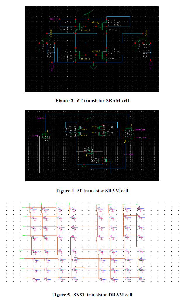
| DRAM stores each bit of data in a separate capacitor within an integrated circuit. The capacitor can be either charged or discharged these two states are taken to represent the two values of a bit, conventionally called 0 and 1. Since capacitors leak charge, the information eventually fades unless the capacitor charge is refreshed periodically. Because of this refresh requirement, it is a dynamic memory as opposed to SRAM and other static memory. The advantage of DRAM is its structural simplicity: only one transistor and a capacitor are required per bit, compared to four or six transistors in SRAM. This allows DRAM to reach very high densities. |
| DRAM is volatile memory (nonvolatile memory) since it loses its data quickly when power is removed. This allows DRAM to reach very high density, Also it consumes less power and is even cheaper than SRAM (except when the system size is less than 8 K) .contents of DRAM are required to be refreshed periodically. By using capacitor there occurs power and delay. By using sense amplifier with multiplexer power consumption and delay reduced when compared to existing one. Proposed design of 4x4 DRAM consumes 11.27mw of power and 8x8 DRAM consumes 37.82mw of power. Calculated delay is 0.39ns for 4x4 DRAM and 1.34ns for 8x8 DRAM. Thus by varying the simulation parameter we achieved our objective. |
References |
|