This paper presents, a high voltage gain DC-DC converter for distributed generation (DG) systems with MPPT controller. A high step-up ratio and clamp- mode converter are proposed to achieve high voltage gain and high efficiency. This can be obtained by using two capacitors and one coupled inductor. During the switch-off period, the capacitors are charged in parallel and during the switch-on period they are discharged in series by the energy stored in the coupled inductor. A passive clamp circuit is used to recycle the leakage inductor energy of the coupled inductor, thus voltage stress on the main switch is reduced. The control method for the circuit is implemented using a MPPT controller which tracks the maximum power of the sources. The converter is suitable for high power applications because of the reduced conduction loss and low input current ripple. The operating principle and MATLAB simulations are discussed in detail.
INTRODUCTION |
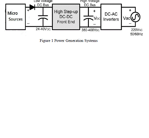
| The distributed generation (DG) systems based on the renewable energy sources have rapidly developed in recent
years.It is a technique that employs small-scale technologies like photovoltaic (PV) cells, fuel cells and wind power to
produce electricity close to the end users of power. Compared to traditional power generators, distributed generators
can provide lower-cost electricity, higher power reliability and security with fewer environmental consequences. But
these are low voltage sources, thus high step-up dc-dc converters with good efficiency are necessary for connecting
these for high voltage applications. To step from low voltage to high voltage, high step-up dc-dc converters are usually
used as the front-end converters which are required to have a large conversion ratio, high efficiency and small volume. |
 |
| Theoretically the conventional boost converter can provide a high step-up voltage gain with a duty cycle greater than
0.9. But in practice, it cannot achieve a high voltage gain with parasitic parameter limitations. Many step-up converters
have been proposed to improve the conversion efficiency. The switched capacitor technique can provide a high step-up
voltage gain, but the conduction loss and voltage stress on the switch is more. The coupled inductor technique can be
used to obtain a high step-up gain, but the conversion efficiency is limited by the leakage inductor Maximum Power Point Tracking is a technique that grid connected inverters, solar battery chargers and similar devices
used to get maximum possible power from one or more photovoltaic devices. The purpose of the MPPT systems is to
sample the output of the cells and apply the proper load to obtain maximum power for any given environmental
conditions. |
MPPT ALGORITHM |
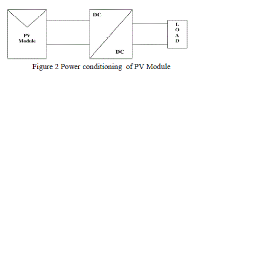
| MPPT algorithms are necessary in PV applications because the MPP of a solar panel varies with the irradiation and
temperature, so the use of MPPT algorithms is required in order to obtain the maximum power from a solar array. Over
the past decades many methods to find the MPP have been developed and published. These techniques differ in many
aspects such as required sensors, complexity, cost, range of effectiveness, convergence speed, correct tracking when
irradiation and/or temperature change, hardware needed for the implementation. |
| Different MPPT techniques |
| 1) Perturb and Observe (hill climbing method) |
| 2) Incremental Conductance method (INC) |
| 3) Fractional short circuit current |
| 4) Fractional open circuit voltage |
| 5) Neural networks |
| 6) Fuzzy logic |
| Nevertheless, the Perturb and Observe (P&O) and Incremental Conductance (INC) techniques are widely used,
especially for low cost implementation. The MPPT algorithm used is Incremental Conductance method (INC). |
 |
| INCREMENTAL CONDUCTANCE |
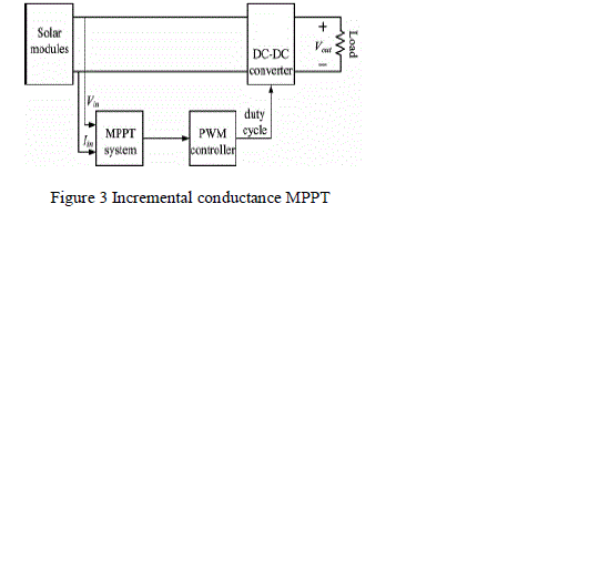
| The theory of the incremental conductance method is to determine the variation direction of the terminal voltage for PV
modules by measuring and comparing the incremental conductance and instantaneous conductance of PV modules. If
the value of incremental conductance is equal to that of instantaneous conductance, it represents that the maximum
power point is found. Incremental conductance method uses voltage and current sensors to sense the output voltage and
current of the PV array. |
 |
PROPOSED SYSTEM |
| The proposed converter combines the switched capacitor and coupled inductor techniques. The switching circuit is
formed by using two capacitors and two diodes are connected to the secondary side of the coupled inductor to achieve a
high voltage gain. Since the voltage across the capacitors can be adjusted by the turns ratio, a high step-up gain can be
achieved. The capacitors are charged in parallel and discharged in series by the coupled inductor. A passive clamp
circuit is used to clamp the voltage level on the switch |
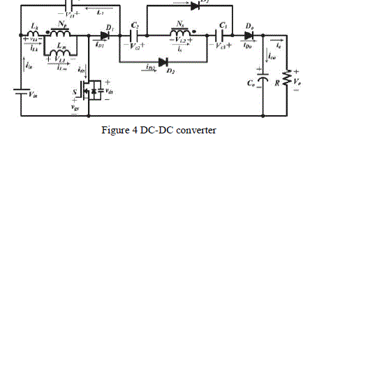 |
| Figure 4 shows the circuit topology of the proposed converter, which is composed of dc input voltage Vin, main switch
S, coupled inductors Np and Ns, one clamp diode D1, clamp capacitor C1, two capacitors C2 and C3, two diodes D2 and
D3, output diode Do, and output capacitor Co. The equivalent circuit model of the coupled inductor includes
magnetizing inductor Lm, leakage inductor Lk, and an ideal transformer. The leakage inductor energy of the coupled
inductor is recycled to capacitor C1 and thus, the voltage across the switch S can be clamped. The voltage stress on the
switch is reduced significantly. Thus, low conducting resistance RDS(ON) of the switch can be used. The proposed
converter combines the concept of switched-capacitor and coupled-inductor techniques. Based on the concept, the
proposed converter puts capacitors C2 and C3 on the secondary side of the coupled inductor. The capacitors C2 and C3
are charged in parallel and are discharged in series by the secondary side of the coupled inductor when the switch is
turned off and turned on respectively. Because the voltage across the capacitors can be adjusted by the turn ratio, the
high step-up gain can be achieved significantly. Also, the voltage stress of the switch can be reduced. The parallelcharged
current is not inrush. Thus, the proposed converter has low conduction loss. Moreover, the secondary-side
leakage inductor of the coupled inductor can alleviate the reverse-recovery problem of diodes, and the loss can be
reduced. In addition, the proposed converter achieves a high step-up gain without an additional winding stage of the
coupled inductor. The coil is less than that of other coupled inductor converters. |
OPERATING PRINCIPLE |
| The main operating principle is that, when the switch is turned on, the coupled-inductor-induced voltage on the
secondary side and magnetic inductor Lm is charged by Vin. The induced voltage makes Vin, VC1, VC2, and VC3 release
energy to the output in series. When the switch is turned off, the energy of magnetic inductor Lm is released via the
secondary side of the coupled inductor to charge capacitors C2 and C3 in parallel. The converter operating in continuous
conduction mode (CCM) is discussed below. In CCM operation, there are five operating modes in one switching
period. The operating modes are described as follows. |
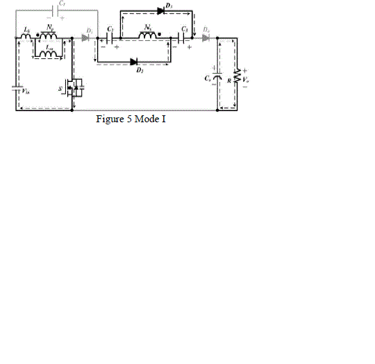
| Mode I : |
| During this mode, S is turned on. Diodes D1 and Do are turned off, and D2 and D3 are turned on. The current-flow path
is shown .The voltage equation on the leakage and magnetic inductors of the coupled inductor on the primary side is
expressed as Vin = VLk+ VLm. The leakage inductor Lk starts to charge by Vin. Due to the leakage inductor Lk, the secondary-side current is of the coupled inductor is decreased linearly. Output capacitor Co provides its energy to load
R. When current iD2 becomes zero, this operating mode ends. |
 |
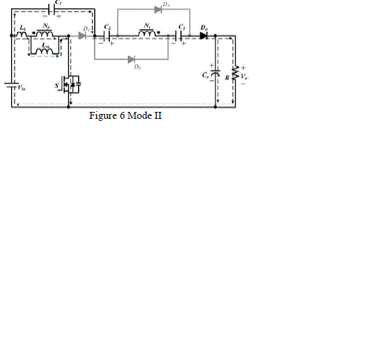
| Mode II : |
| During this time interval, S remains turned on. Diodes D1, D2, and D3 are turned off, and Do is turned on. The currentflow
path is shown. Magnetizing inductor Lm stores energy generated by dc source Vin. Some of the energy of dc-source
Vin transfers to the secondary side via the coupled inductor. Thus, the induced voltage VL2 on the secondary side of the
coupled inductor makes Vin, VC1, VC2, and VC3, which are connected in series, discharge to high-voltage output capacitor
Co and load R. This operating mode ends when switch S is turned off . |
 |
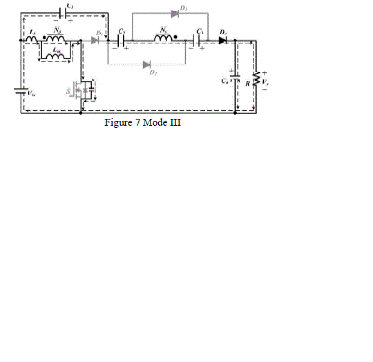
| Mode III |
| During this time interval, S is turned off. Diodes D1, D2, and D3 are turned off, and Do is turned on. The current-flow
path is shown. The energies of leakage inductor Lk and magnetizing inductor Lm charge the parasitic capacitor Cds of
main switch S. Output capacitor Co provides its energy to load R. When the capacitor voltage VC1 is equal to Vin + Vds
diode D1 conducts, and this operating mode ends. |
 |
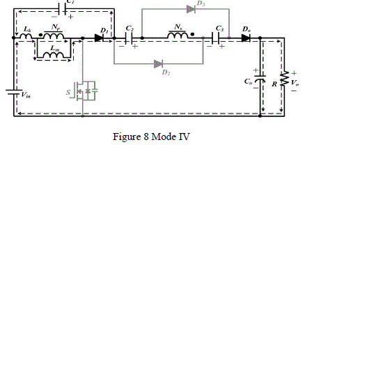
| Mode IV : |
| During this time interval, S is turned off. Diodes D1 and Do are turned on, and D2 and D3 are turned off. The currentflow
path is shown .The energies of leakage inductor Lk and magnetizing inductor Lm charge clamp capacitor C1. The
energy of leakage inductor Lk is recycled. Current iLk decreases quickly. Secondary-side voltage VL2 of the coupled
inductor continues charging high-voltage output capacitor Co and load R in series until the secondary current of the coupled inductor is is equal to zero. Meanwhile, diodes D2 and D3 start to turn on. When iDo is equal to zero this
operating mode ends. |
 |
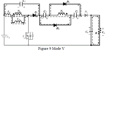
| Mode V : |
| During this time interval, S is turned off. Diodes D1, D2 and D3 are turned on, and Do is turned off. The current-flow
path is shown. Output capacitor Co is discharged to load R. The energies of leakage inductor Lk and magnetizing
inductor Lm charge clamp capacitor C1. Magnetizing inductor Lm is released via the secondary side of the coupled
inductor and charges capacitors C2 and C3. Thus, capacitors C2 and C3 are charged in parallel. |
 |
BASIC SIMULATION |
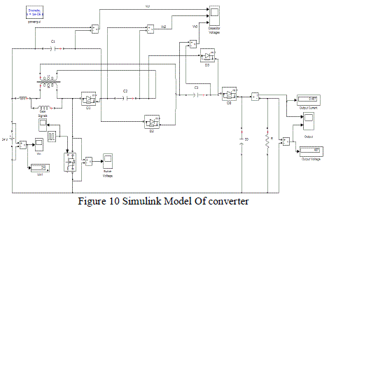
| The converter was simulated with MATLAB software. |
 |
 |
 |
 |
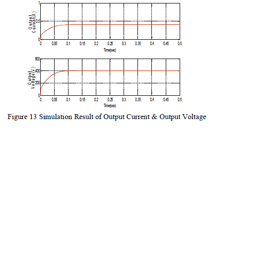 |
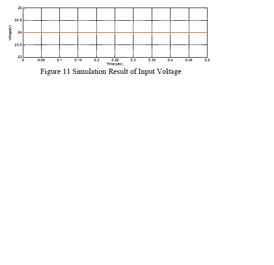
| The DC-DC converter was simulated for an input of 24V and a load resistance of 1kΩ .The output voltage was
obtained as 400V. |
| PV SIMULATION WITH MPPT CONTROLLER |
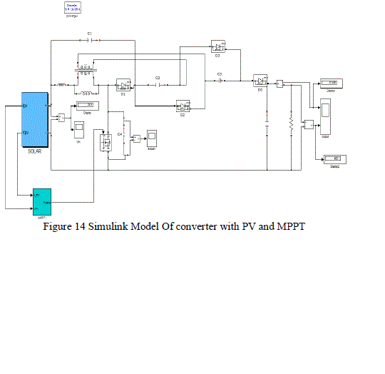
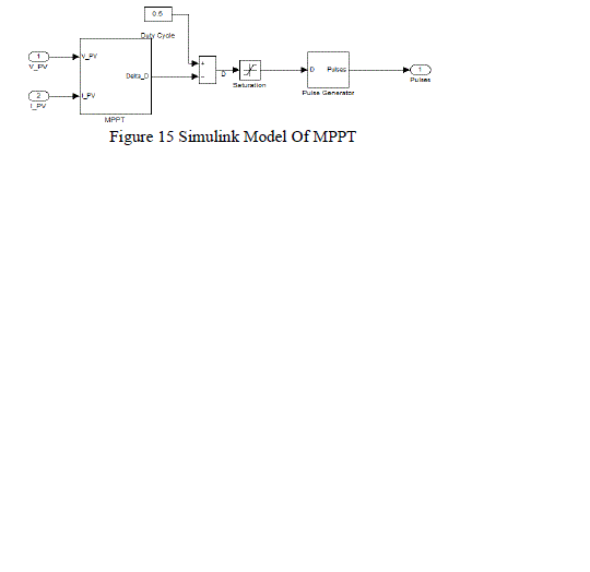
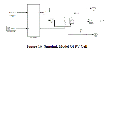
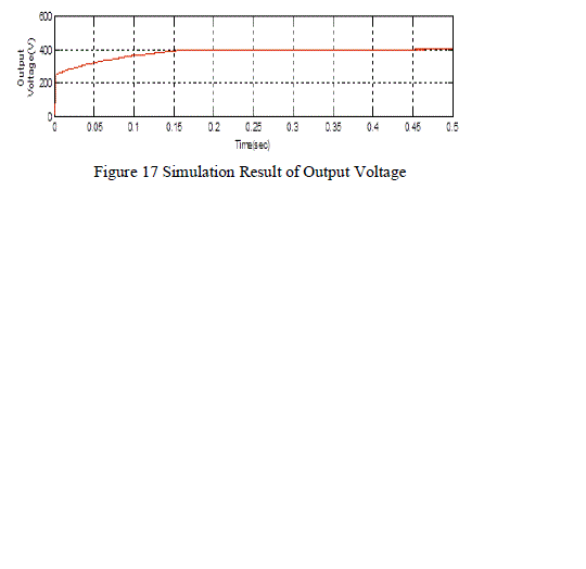
| The converter can be used for distributed generation systems so it is simulated in MATLAB software with a
photovoltaic array as input. MPPT controller is used to get the maximum output. The simulink model of the system is
shown in figure 14.The output voltage was obtained as 400V. |
 |
 |
 |
 |
EXPERIMENTAL RESULTS |
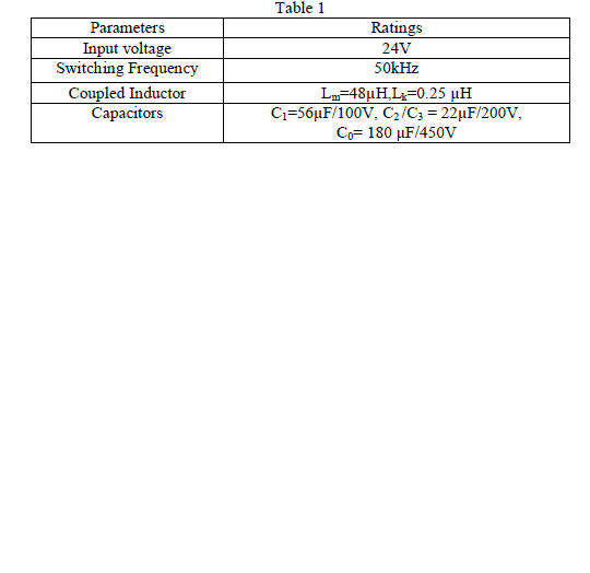
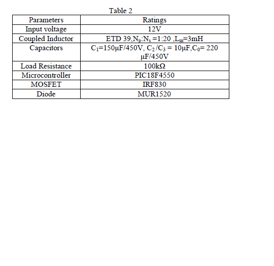
| A prototype of the converter with following specifications has been implemented. |
 |
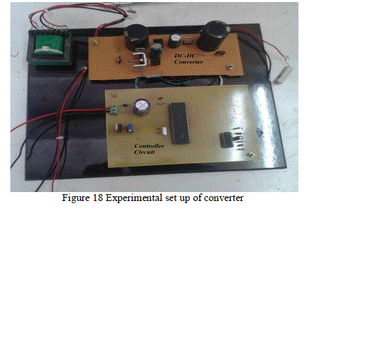 |
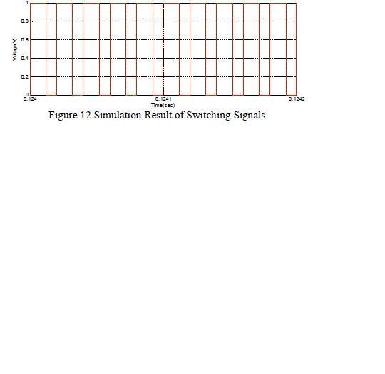
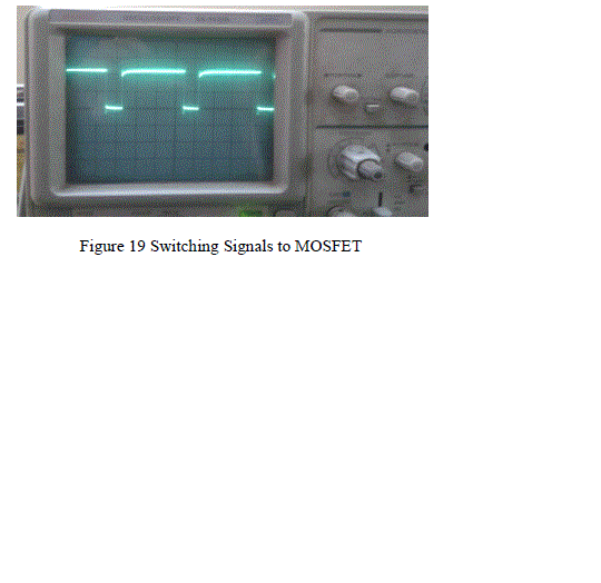
| A 5V power supply is given to the PIC microcontroller for generating the gating signals to the MOSFET. The gating
signals are given to the MOSFET through MOSFET driver. An input voltage of 12V was applied to the converter using
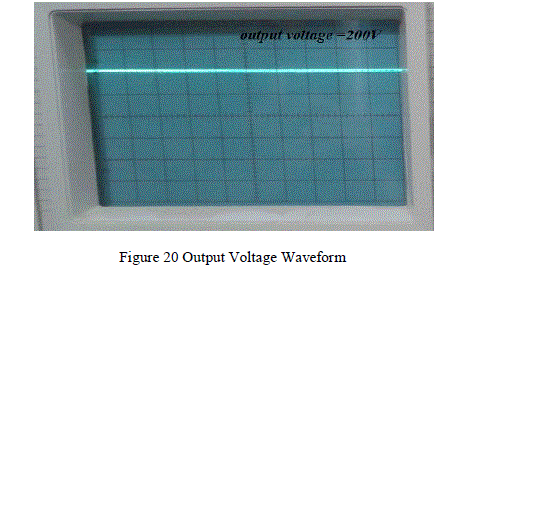
a battery.The switching signals to the MOSFET are generated at a frequency of 50kHz.An output voltage of 200V was
obtained.The converter was also connected to a PV panel and the output voltage was verified. The switching signals are
as shown in Figure 19. |
 |
| The output was verified using a CRO. The output waveform is as shown in Figure 20. |
 |
CONCLUSION |
| In this paper a high step-up dc-dc converter for distributed power generation is discussed. By using the capacitor
charged in parallel and discharged in series by the coupled inductor this converter provide high step-up voltage gains
and high efficiency. It also has low input current ripple and low conduction losses, making it suitable for high power
applications. The turn ratio of the coupled inductor is 1:4, but the output voltage of the converter is 16 times greater
than the input voltage. The converter transfers the capacitive and inductive energy simultaneously to increase the total
power delivery. |
References |
- M.M.Jovanovic ,andY. Jang, âÃâ¬ÃËA new soft-switched boost converter with isolated active snubberâÃâ¬Ãâ¢, IEEE Trans. Ind. Appl., pp. 496âÃâ¬Ãâ502, March 1999
- N. P. Papanikolaou and E. C. Tatakis, âÃâ¬ÃÅActive voltage clamp in flyback converters operating in CCM mode under wide load variation,âÃâ¬Ã IEEE Trans. Ind. Electron., vol. 51, no. 3, pp. 632âÃâ¬Ãâ640, Jun. 2004.
- Q. Zhao, F. Tao, Y. Hu, and F. C. Lee, âÃâ¬ÃÅActive-clamp DC/DC converter using magnetic switches,âÃâ¬Ã in Proc. IEEE Appl. Power Electron. Conf. Expo, pp. 946âÃâ¬Ãâ952., April 2001
- B. R. Lin and F. Y. Hsieh, âÃâ¬ÃÅSoft-switching zetaâÃâ¬Ãâflyback converter with a buckâÃâ¬Ãâboost type of active clamp,âÃâ¬Ã IEEE Trans. Ind. Electron., vol. 54, no. 5, pp. 2813âÃâ¬Ãâ2822, Oct. 2007.
- B. Axelrod, Y. Berkovich, and A. Ioinovici, âÃâ¬ÃÅSwitched-capacitor/switched-inductor structures for getting transformerless hybrid dcâÃâ¬Ãâdc PWM converters,âÃâ¬Ã IEEE Trans. Circuits Syst. I, Reg. Papers, vol. 55, no. 2, pp. 687âÃâ¬Ãâ696, Mar. 2008.
- Da Silva, E.S., Dos Reis Barbosa, L., Vieira, J.B., De Freitas, L.C., and Farias, V.J.: âÃâ¬ÃËAn improved boost PWM soft-single-switched converter with low voltage and current stressesâÃâ¬Ãâ¢, IEEE Trans. Ind.Electron., 48, (6), pp. 1174âÃâ¬Ãâ1179,2001
- Roh, C.W., Han, S.H., and Youn, M.J.: âÃâ¬ÃËDual coupled inductor fed isolated boost converter for low input voltage applicationsâÃâ¬Ãâ¢, Electron.Lett., 35, pp. 1791âÃâ¬Ãâ1792,1999
- Q. Zhao and F. C. Lee, âÃâ¬ÃÅHigh-efficiency, high step-up dcâÃâ¬Ãâdc converters,âÃâ¬Ã IEEE Trans. Power Electron., vol. 18, no. 1, pp. 65âÃâ¬Ãâ73, Jan. 2003.
- L. Huber and M. M. Jovanovic, âÃâ¬ÃÅA design approach for server power supplies for networking,âÃâ¬Ã Proc. IEEE Applied Power Electronics Conf.APECâÃâ¬Ãâ¢00, vol. 2, pp. 1163âÃâ¬Ãâ1169, Feb. 2000.
- R. J. Wai, C. Y. Lin, C. Y. Lin, R. Y. Duan, and Y. R. Chang, âÃâ¬ÃÅHigh efficiency power conversion system for kilowatt-level stand-alone generation unit with low input voltage,âÃâ¬Ã IEEE Trans. Ind. Electron., vol. 55, no. 10, pp. 3702âÃâ¬Ãâ3714, Oct. 2008.
- M. Lokhanadham , K. VijayaBhaskar ,âÃâ¬ÃÂIncremental Conductance Maximum Power Point Tracking(MPPT) for Photovoltaic System ,âÃâ¬ÃÂInternational Journal of Engineering Research Application, vol. 2,no. 2,pp 1420-1424,Jan 2009
- NehaAdhikari, BhimSingh ,A.L.Vyas âÃâ¬ÃÅPerformance Evaluation of a Low Power Solar PV Energy System With Sepic converter,âÃâ¬Ã IEEE PEDS, Dec 2011
- S. K. Changchien, T. J. Liang, J. F. Chen, and L. S. Yang, âÃâ¬ÃÅNovel high step-up dcâÃâ¬Ãâdc converter for fuel cell energy conversion system,âÃâ¬Ã IEEE Trans. Ind. Electron., vol. 57, no. 6, pp. 2007âÃâ¬Ãâ2017, Jun. 2010
- SurinBor-RenLin,Chien-Lan Huang and Jin âÃâ¬ÃâFa Wan,âÃâ¬Ã Analysis ,Design , and Implementation of a Parallel ZVS Converter,âÃâ¬ÃÂ. IEEE Trans. Ind. Electron, vol 55, no. 4, pp. 1586-1594, April 2008.
- M. G. Villalva, J. R. Gazoli, E. RuppertF..âÃâ¬ÃÂModelingAnd Circuit-Based Simulation Of Photovoltaic ArraysâÃâ¬Ã Brazilian Journal of Power Electronics, vol.14, no. 1, pp. 35-45, July 2009
- Azadeh Safari and SaadMekhilef, âÃâ¬ÃÅSimulation and Hardware Implementation of Incremental Conductance MPPT With Direct Control Method Using Cuk ConverterâÃâ¬ÃÂ, IEEE Trans. Ind. Electron., vol. 58, no. 4, pp.1154-1161, Apr. 2011.
|