Generally conventional boost converters have been used to obtain higher output voltage than the input voltage. When these boost converters are operated for high ratios it leads to high voltage and current stress on the switch. Hence an interleaving technique of boost converter has been presented. This method of approach can be used in high power applications to produce high voltage gain when compared to the conventional boost converter. Two different interleaved boost converter topologies have been discussed for better performance. The input is solar source with MPPT has been used to track the maximum power and utilize in an efficient manner
Keywords |
| Interleaved boost converter, Maximum power point tracking, Photovoltaic system, Duty cycle, Perturb &
Observe. |
INTRODUCTION |
| In general various DC-DC converter topologies have been used in the energy systems. Irrespective of their differences
they all try to input the maximum amount of power from the system with as little loss of energy as possible within the
circuit itself. DC-DC converter is a switching converter which inherently introduces a certain amount of ripple in the
current thereby reducing the efficiency. Usually this ripple is minimized by using a filter at the output terminals. While
this is a solution, the magnitude, cost and life of the filter dependent on the types of converter used. Converters are
based on buck, boost, buck-boost and cuk are derived topologies. Here boost converter with an interleaving technique
has been discussed for two different topologies to obtain a high voltage gain. The different topologies implemented
gives difference in their output. |
LITERATURE SURVEY |
| A parallel connection technique of boost converter for unity power factor was proposed in [1]. This system is based on
two cell converter which is operated in continuous inductor current mode. With an extra small inductance, two
MOSFET pulse width modulation are connected in parallel, which provides an increased output power. Any number of
PWM cells can be paralleled by this method. DC to DC switching converters with parallel connection of N-identical
boost converters with Current-Mode Control (CMC) is presented in [2]. The CMC helps to reduce the ripple of the total
input current and output voltage operating with same duty cycle. Here no use of eternal triangular or sawtooth signals is
required. A converter with two interleaved and intercoupled boost converters has been proposed in [3]. This method
helps in equal current sharing between two parallel connection boost converters. The analysis of interleaved boost
converter has been compared with the conventional boost converter. Two boost converters in interleaved operation
named, Interleaved Dual Boost (IDB) and Switched Capacitor Interleaved Dual Boost (SCIDB) has been presented in
[4]. This interleaved boost converter under sliding mode control is analyzed in this paper. This interleaving technique
results in a step-up structure. Interleaved boost converter with the use of zero current transition and a soft commutation
technique operating in Critical Conduction Mode (C-DCM) was investigated in [5]. The turn-ON of the main switches
occurs naturally at ZCS due to the operation of C-DCM and also the reverse recovery losses of the diodes are
minimized. The circuit of the converters has been implemented by using a single Erasable Programmable Logic Device
(EPLD). A Coupled-Inductor Interleaved Boost Converter (CIBC) fed PV system using a fuzzy controller with a
feedforward MPPT scheme was developed in [6]. This system has low switch current loss and improves efficiency than
the noncoupled converter system. For the given solar insolation the tracking algorithm changes the duty ratio of the
converter so that the solar cell array voltage equals the voltage corresponding to the MP point. |
| A novel ZCS-PWM boost rectifier has been presented in [7]. This circuit is used to achieve nine transition states in the
power conversion and PFC. The rectifier has been built with state-space average model. The ZCS usage in the rectifier
provides high efficiency. A two-inductor, interleaved power-factor corrected boost converter exhibiting voltage doubler
characteristics when the duty cycle is greater than 0.5 was introduced in [8]. This voltage doubler characteristic of the
converter is suitable for universal-line (90-264 VRMS). Since the proposed PFC boost rectifier operates as voltage
doubler at low-line, its efficiency is improved compared to the conventional boost converter. A new technique of
interleaved boost converter with coupled inductors and switched capacitors was proposed in [9]. This technique is
added to the output stage so that higher step-up voltage gain and lower voltage stress is obtained when compared to
conventional interleaved boost converter. Hence low-conduction resistance and low-voltage rated switches can be
applied. The load-current can be equally shared by each phase without any additional current sharing module. The
switching losses can be reduced by the ZVT soft switching performance. An active clamped circuit adopted also helps
in the reduction of switching losses and the leakage energy of the coupled inductor is recycled. A new dual interleaved
active-clamp forward topology has been proposed in [10]. Series and parallel connection of two interleaved forward
circuits on the primary and secondary side respectively. This proposed method provides a new solution to reduce the
voltage stress and number of components. An interleaved boost converter with soft switching technique and modelling
of PV topology with MPPT controller was proposed in [11]. This interleaved boost converter has been used to increase
the output power in high power applications. This interleaved boost converter required low current rating of switching
device since the current in each phase is distributed. An interleaving boost converter with PV and a passive snubber for
battery charging applications was introduced in [12]. The snubber helps to reduce the voltage stresses at turn-off
transition and to obtain maximum power P&O method is used. A interleaved boost converter which is magnetically
coupled to a voltage doubler circuit, providing a voltage gain higher than that of conventional boost converter was
discussed in [13]. This converter has low voltage stress across the switch, voltage balancing between output capacitors,
low input-current ripple, and high switching frequency. |
| A soft switching interleaved boost converter containing two shunted elementary boost conversion units and an auxillary
inductor was implemented in [14]. This converter turns ON both the active power switches at their zero voltage to
reduce switching losses and raise the conversion efficiency. This identical design of the boost converter helps for a
sample design. A comparison between conventional boost converter and interleaved PFC boost converter was
investigated in [15]. The comparison is made for identical conditions and the performance has been evaluated. These
results provide a better performance for interleaved PFC boost converter resulting in higher efficiency and low THD
values. Thus two main PFC boost converters are investigated for lithium-ion battery has been used in electrical cars.
Interleaved boost converter with two different topology has been considered. Topology 1 has been operated to obtain
high voltage gain and topology 2 also works for higher voltage gain than the topology 1. Here both the topology has
been fed with a solar model as input source. |
MATHEMATICAL MODEL |
| The PV panel mathematical model can be represented as shown in Fig. 1 |
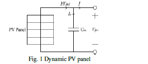 |
| The equations that describe the electric behavior of the PV panel under constant irradiance and temperature are, |
 |
| The output current of the PV panel is taking to be equal to the average input current of the DC-DC converter. The
maximum power of the PV panel is given by, |
 |
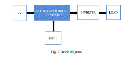
| The block diagram of an interleaved boost converter is shown in Fig. 2, |
 |
PROPOSED METHODOLOGY |
| This paper compares the operation of two different topologies of interleaved boost converter. The proposed topology
contains the interleaved boost converter with solar as linear model. Also the interleaved boost converter of proposed
topology has been worked with an MPPT to obtain maximum output. The conventional interleaved boost converter is
coupling many stages of a boost converter to obtain high voltage gain. The proposed method is different from the
conventional interleaved boost converter as its position of the inductors and capacitors are changed to obtain high
voltage gain. The circuit diagram of topology 1 is shown in Fig. 3 |
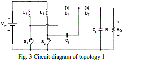 |
| The circuit operation of topology 1 is explained in the following modes, |
| Mode (i) |
| When both the switches are turned ON with a duty cycle less than 0.5, the inductor current of the inductors L1 and
L2 rises linearly and stores energy. The output voltage is similar to the input voltage. The ratio of output voltage to
input voltage can be given as follows, |
 |
| Mode (ii) |
| When both the switches are turned ON with a duty cycle greater than 0.5 to 1, the inductor current of the inductors
L1 and L2 rises linearly with the output voltage greater than the input voltage. The ratio of output voltage to input
voltage can be given as follows, |
 |
| Fig. 4 shows the circuit diagram of topology 2. |
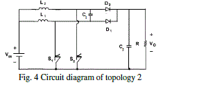 |
| The circuit operation of topology 2 is explained in the following modes, |
| Mode (i) |
| When both the switches are turned ON with a duty cycle less than 0.5, the inductor current of the inductors L1 and
L2 rises linearly with the input voltage and hence the output voltage is higher than the input voltage. |
| Mode (ii) |
| When both the switches are turned ON operating with a duty cycle greater than 0.5 to 1, the inductor L1 and L2
charges with the input and hence the output voltage is higher than the input voltage. |
MPPT SYSTEM |
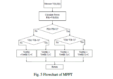
| The MPPT technique used here is P&O method. This method measures the value of voltage and current and from that
the power can be calculated. The calculated power is checked for greater value by making a comparison with the
previous power value. If the calculated power value is greater than the previous value then similarly the voltage value is
made a comparison with the present and previous value. If the voltage is also greater than the previous value then the
reference value is taken as the previous voltage with an increment of constant value otherwise the reference is taken as
the previous voltage value with a decrement of constant value. It can be represented as a flowchart as shown in Fig. 5, |
 |
SIMULATION RESULTS |
| The circuit of both the topology has been designed in MATLAB/simulink with the help of the blocks available in the
simulink library. The simulation diagram of topology 1 is represented in Fig. 6 |
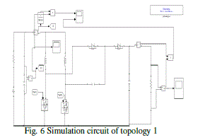 |
| Fig. 6 shows the simulation of topology 1 with the solar as liner model to obtain high voltage gain. |
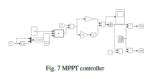
| The MPPT controller of the both the topologies has been designed with the help of P&O algorithm which has been
implemented in Matlab/simulink. This MPPT controller designed is used to track the maximum power at different
points and adjust to the path where there is maximum power. The implementation of the MPPT can be obtained as
shown in Fig. 7 |
 |
| The simulation diagram of topology 2 is as shown in Fig. 8 |
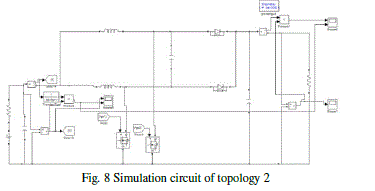 |
| Fig. 8 represents the simulation of topology 2 with solar as linear model so that high voltage gain could be obtained.
The simulation results obtained for the different topology is shown as follows. The parameters taken are input
voltage=5 V, duty cycle=50 %, frequency=25 kHz which are common for both the topologies. The topology 1 provides
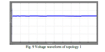
the output voltage of 16.29 V and topology 2 provides 18.59 V. The output voltage waveform of topology 1 and
topology 2 are as shown in Fig. 9 and Fig. 10 respectively. |
 |
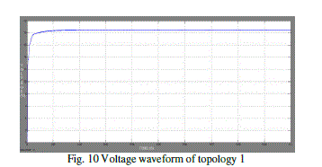 |
| Fig. 9 and Fig.10 are the waveforms obtained are from a solar linear model with MPPT for an interleaved boost
converter topology and hence the output is also DC. The waveform reveals the operation of the interleaved boost
topologies working for high voltage gain. |
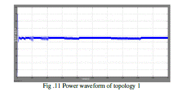
| The power waveform of topology 1 and topology 2 obtained for input voltage=5 V, duty cycle=50 %, frequency=25
kHz, the power waveform of topology 1 and topology 2 are as shown respectively in Fig. 11 and Fig. 12. |
 |
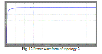 |
| The output power waveforms obtained from solar linear model with MPPT for the interleaved boost converter
topologies shows that the power is tracked at the point where maximum power is present. The waveform rises at the
initial point and then it is maintained constantly as the converter is similar to that of a boost converter.
The PV power and PV voltage characteristics obtained for a solar linear model of 100 W panel can be represented as
shown in Fig. 13 and Fig. 14 respectively. |
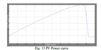 |
| The above obtained curve explains that the power obtained for changes in irradiation changes the maximum power
point towards the right hand side of the curve. The algorithm takes a change due to perturbation and in the next stage it
changes the direction of perturbation and goes away from the maximum point. The curve is linearly rising from the
initial part to the maximum power point and then it falls down steeply. |
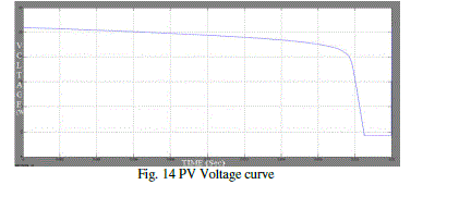 |
| The voltage curve obtained is for the maximum power tracking point. This curve depends on the irradiation of the
panel. The PV voltage curve shows that it is maintained constant for a certain period and then it gradually decreases
with respect to time. |
| A comparison has been made for two different topologies with a conventional boost converter so that the better
performance of the topologies can be concluded. |
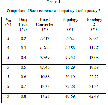 |
| The obtained comparison result has been plotted in Fig. 15 as shown below, |
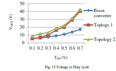 |
| The comparison clearly reveals that topology 2 operations gives better performance compared to the conventional boost
and topology 1. |
CONCLUSION |
| It is obtained that the different topology operation of interleaved boost converter is simulated and the results revealed
shows that the topology 2 with MPPT can be operated for better performance. |
References |
- H. A. C. Braga and I. Barbi, âÃâ¬ÃÅA 3-kw unity-power-factor rectifier based on a two-cell boost converter using a new parallel-connection technique,âÃâ¬Ã IEEE Trans. Power Electron., vol.14, no.1, pp.209-217, Jan.1999.
- R. Giral, L. M. Salamero, and S.Singer, âÃâ¬ÃÅInterleaved converters operation based on CMC,âÃâ¬Ã IEEE Trans. Power Electron., vol.14, no.4, pp. 643-652, Jul.1999.
- P. W. Lee, Y. S. Lee, D. K. W. Cheng, and X. C. Liu, âÃâ¬ÃÅSteady-state analysis of an interleaved boost converter with coupled inductors,âÃâ¬Ã IEEE Trans. Ind. Electron., vol.47, no.4, pp.787-795, Aug.2000.
- Roberto Giral, Luis Martinez-Salamero, Ramon Leyva and Javier Maixe, âÃâ¬ÃÅSliding-Mode control of interleaved boost converters,âÃâ¬Ã IEEE Trans. on circuits and systems-I: Fundamental theory and applications, vol.47, no.9, pp.1330-1339, Sep.2000.
- C. M. O. Stein, J. R. Pinheiro, and H. L. Hey , âÃâ¬ÃÅA ZCT auxiliary commutation circuit for interleaved boost converters operating in critical conduction mode,âÃâ¬Ã IEEE Trans. Power Electron., vol.17, no.6, pp.954-962, Nov.2002.
- M. Veerachery, T. Senjyu, and K. Uezato,âÃâ¬ÃÅNeural-network-based maximum-power-point tracking of coupled-inductor interleaved boost converter- supplied PV system using fuzzy controller,âÃâ¬Ã IEEE Trans. Ind. Electron., vol.50, no.4, pp.749-758, Aug.2003.
- Chien-Ming Wang, âÃâ¬ÃÅA new single-phase ZCS-PWM boost rectifier with high power factor and low conduction losses,âÃâ¬Ã IEEE Trans on Ind. Electron., vol.53, no.2, pp.500-510, Apr.2006.
- Yungtaek Jang, and Milan M. Jovanovic, âÃâ¬ÃÅInterleaved boost converter with intrinsic voltage-doubler characteristics for universal-line PFC front end,âÃâ¬Ã IEEE Trans. on Power Electronics, vol.22, no.4, pp.1394-1401, Jul.2007.
- Ting Qian and Brad Lehman, âÃâ¬ÃÅDual interleaved active-clamp forward with automatic charge balance regulation for high input voltage applications,âÃâ¬Ã IEEE Trans. on Power Electronics, vol.23, no.1, pp.38-44, Jan.2008.
- Dong Wang, Xiangning He, and Rongxiang Zhao, âÃâ¬ÃÅZVT interleaved boost converters with built-in voltage doubler and current auto-balance characteristic,âÃâ¬Ã IEEE Trans. on Power Electronics, vol.23, no.6, pp.2847-2854, Nov.2008.
- M. Marimuthu, A. Kamalakannan and M. Karthick, âÃâ¬ÃÅInterleaved boost converter with MPPT controller for photovoltaic system,âÃâ¬Ã MIT International Journal of Electrical and Instrumentation Engg, vol.2, no.2, pp.70-76, Aug.2012.
- Sheng-Yu Tseng, and Cheng-Tao Tsai, âÃâ¬ÃÅPhotovoltaic power systems with an interleaving boost converter for battery charger applications,âÃâ¬Ã International Journal of Photoenergy, vol. 2012, 15 pages, Sep.2012.
- Gustavo, A. L. Henn, R. N. A. L. Silva, Paulo P. Praca Luiz H. S. C. Baretto, and Demercil S. Oliveira, Jr. âÃâ¬ÃÅInerleaved boost converter with high voltage gain,âÃâ¬Ã IEEE Trans. on Power Electrons, vol.25, no.11, pp.2753-2761, Nov.2010.
- Vaddi Ramesh, U. Haribabu, âÃâ¬ÃÅSimulate the implementation of interleaved boost converter with zero voltage transition,âÃâ¬Ã International Journal of Engg Research and Applications, vol.2, no.6, pp.1129-1135, Nov-Dec.2012.
- Burak Akin, âÃâ¬ÃÅComparison of conventional and interleaved PFC boost converters for fast and efficient charge of Li-ion batteries used in electrical cars,âÃâ¬Ã International Conference on Power and Energy Systems, vol.13, pp.499-504, 2012.
|