International Journal of Advanced Research in Electrical, Electronics and Instrumentation Engineering
ISSN ONLINE(2278-8875) PRINT (2320-3765)
ISSN ONLINE(2278-8875) PRINT (2320-3765)
Anupama B R1, M C Chandrashekhar2 and Dr. M Z Kurian3
|
| Related article at Pubmed, Scholar Google |
Visit for more related articles at International Journal of Advanced Research in Electrical, Electronics and Instrumentation Engineering
One of the advance modulation method is the Minimum Shift Keying (MSK), but it potentially creates sidebands, that extending out a long way from the carrier, causes interference to adjacent channels and any radio communications links that may be using them. To avoid interference Gaussian Minimum Shift Keying (GMSK) modulation scheme is used in this project, input is filtered using Gaussian filter before modulation, which takes large resources to implement on FPGA. By taking advantage of the Xilinx FPGA look-up table architecture, the Distributed Algorithm (DA) is used to implement the Gaussian filter, algorithm performs multiplication with look-up table method. So that low power, high spectrum efficient communication system is developed. Modulation is carried out using Discrete Frequency Synthesizer (DFS), which has multiplier less structure, utilizes less resource on FPGA.
Keywords |
| MSK, GMSK, FPGA, DA, DFS |
INTRODUCTION |
| In wireless communication system, it must has the system design such that, which meet the delay reduction, area optimization and power efficiency, using available resources with the less cost, so can use FPGA to implement the system design to meet all these criteria. Modulation and demodulation are the most important aspect in the communication, so have to choose an effective method to implement. One of the techniques for occupying less bandwidth and power, Gaussian Minimum Shift Keying (GMSK) modulation scheme [1] is used in the project and it also has advantages of being able to carry digital modulation while still using the spectrum efficiently and there is no sidebands extend outwards from the main carrier and hence there is no interference to other radio communications systems using nearby channels. GMSK is derived from Continuous Phase Frequency Shift Keying Method (CPFSKM) by selecting the frequency deviation to be the minimum possible and filtering the baseband modulating signal with a Gaussian filter. All this is to be done to minimize the spectrum width of the signal. |
| To achieve all these criteria on communication system requires large recourses on FPGA, to reduce the area on Field Programmable Gate Array (FPGA), Distributed Algorithm or Distributed Arithmetic Algorithm (DA) is used. DA is a computation algorithm that performs multiplication with look-up based scheme, which is inspired by the potential of the Xilinx FPGA look-up table architecture. DA specifically targets the sum of products computation that covers many of the important DSP filtering and frequency transforming functions. So that the advantages GMSK modulation method can be utilized in a number of wireless communications applications such as GSM and EDGE technologies etc. The modules (transmitter and receiver) is describe using VHDL and implemented on the Spartan 3E FPGA. |
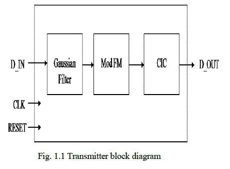
| There are only a few known implementations of this kind of systems on FPGA [1] [2] [3] [4]. To make this design very useful for future developments, the entire system is developed with modular blocks interconnected [1], using input and output enable control signals. Fig. 1.1 shows the transmitter block diagram, input is given to Guassian filter which romoves noice and avoides interference with other signals. The output of the Guassian filter is passed for modulation, Discrete Frequecny synthesizer (DFS) modulates the incoming binary data, two different carrier frequencies are generated for „0âÃâ¬ÃŸ and „1âÃâ¬ÃŸ. The generated carrier signal frequency is increased using Cascade Integrate Combs (CIC) filter, which acts as a upsampler in transmitter part to avoid aliasing effect. Finally tansmitter part sends the signal to receiver. |
 |
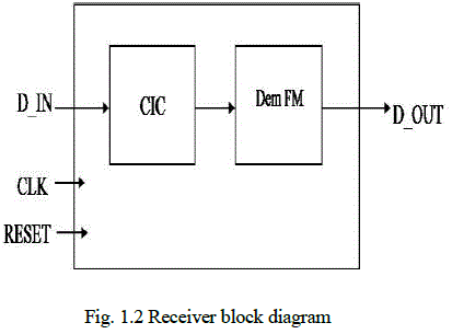
| Fig. 1.2 shows the block diagram of receiver. CIC filter reduces the sample rate of the received signal. From Dem FM can obtain transmitted digital data back where DFS compares the incoming signal with two different carrier frequencies and identifies the digital signal as „0âÃâ¬ÃŸ or „1âÃâ¬ÃŸ. |
 |
DISTRIBUTED ALGORITHM |
| Distributed Algorithm or Distributed Arithmetic (DA) plays a important role in embedding DSP functions in the Xilinx 4000 family of FPGA devices. Distributed arithmetic, along with Modulo Arithmetic, are computation algorithms that performs multiplication using look-up table based method. DA specifically targets the sum of products (also referred to as the vector dot product) computation that covers many of the important DSP filtering and frequency transforming functions. The arithmetic sum of products that defines the response of linear, time invariant network can be expressed as |
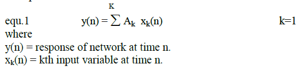 |
| Ak = weighting factor of kth input variable that is constant for all n, and so it remains time-invariant. |
| Ak, are the filter coefficients, here Gaussian coefficients are considered and xk,, are the variables from prior samples of a single data source (for example, from an analog to digital converter output). In frequency transforming mothod whether the discrete Fourier or the fast Fourier transformation, the constants are the sine or cosine basis functions and the variables are a block of samples from a single data source. Multiple data sources can be found using image processing. From equation 1 can observe that a single output response requires the accumulation of K product terms. Using DA method the summing of product terms is replaced by look-up table procedure that are easily implemented in the Xilinx Configurable Logic Block (CLB) look-up table architecture. |
| The number format of the variable is defined in 2âÃâ¬ÃŸs complement, fractional - a standard practice for fixedpoint microprocessors in order to bound number growth under multiplication. As is the case of microprocessor constant Ak, needs no restriction, nor are they required to be matched with the data word length. The constants may have a mixed format of both integer and fraction. The variable xk, may be written in the fractional format as shown in equation 2. |
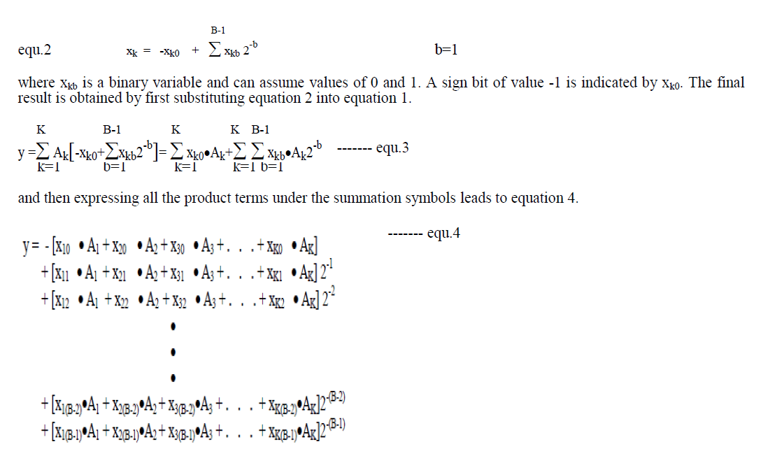 |
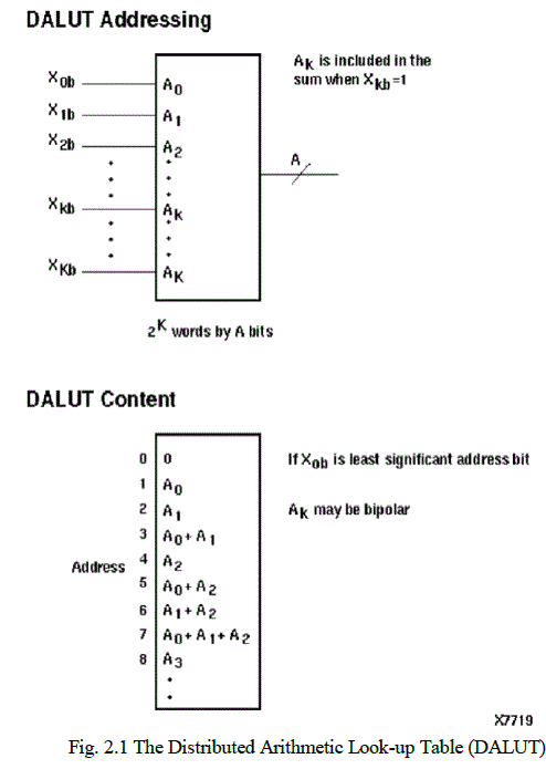
| Each term within the brackets represent a binary AND operation involving a bit of the input variable and all the bits of the filter coefficient and signs represents arithmetic sum operations. The exponential term denote the scaled contributions of the bracketed pairs to the total sum. A look-up table is constructed that can be addressed by the same scaled bit of all the input variables and can access the sum of the terms within each pair of brackets. Such a table is shown in Fig. 2.1 and therefore referred to as a Distributed Arithmetic look-up table or DALUT. The arithmetic operations have now been reduced to just an addition, subtraction, and binary scaling. |
 |
DISCRETE FREQUENCY SYNTHESIZER |
| Digital frequency synthesizer is used to generate a sampled sinusoidal wave in many DSP tasks. DFS has advantage that the its output frequency, phase and amplitude can be precisely and rapidly controlled. DFS also has the ability to tune with extremely fine frequency and phase resolution and to rapidly “hop” between the frequencies. All these characteristics have made this technology popular in radar, military and communications systems. There are different approaches are available to produce sine wave, one of the popular technique is the CORDIC algorithm [5], which uses an iterative computation method to produce sine wave. But circuit complexity and distortions will be generated, when the memory compression is employed and also canâÃâ¬ÃŸt change the carrier frequency once itâÃâ¬ÃŸs defined. |
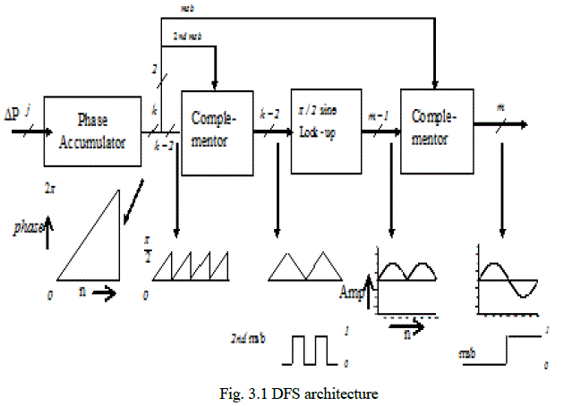 |
| The DFS in a simplified form is shown in the Fig. 3.1 It consists of a phase accumulator and a phase to amplitude converter (conventionally a sine ROM) [14]. The phase accumulator produce a linearly increasing phase value. Every value at the output of the phase accumulator is converted to approximated sine amplitude by a phase-to-sine amplitude converter, which is implemented using Read Only Memory (ROM) is a look-up table which converts the digital phase information into the values of a sine wave. The spectral purity of the DFS is achieved by the values stored in the sine table ROM. Hence, can increase the resolution of the ROM. But as ROM storage increases the power consumption is higher, lower speed and greatly increased costs. |
| The most elementary technique of compression is to store only π/2 radians of sine wave information and to generate the ROM samples for the full range of 2π by exploiting the quarter wave symmetry of the sine function. Look-up table capacity is decreased by the additional logic, which is necessary to generate the complements of the accumulator and the look-up table output. The two most significant bits are used to decode the quadrant and the remaining k-2 bits are used to address a one-quadrant sine table look-up. The most significant bit determines whether the amplitude is increasing or decreasing. The accumulator output is used “as is” for the first and the third quadrants. The bits must be complemented so that the slope of the saw-tooth is inverted for the second and fourth quadrant. As shown in the Fig. 3.1, the sampled waveform at the output of the look-up table is a full wave rectified version of the desired sine wave. The final output sine wave is then generated by multiplying the full wave rectified version by -1, when the phase is between π and 2π . |
| Two different carrier frequencies are generated for modulation for bit „0âÃâ¬ÃŸ and „1âÃâ¬ÃŸ. At the receiver part the received frequency is identified to obtain the digital data back using same DFS architecture. |
IMPLEMENTATION RESULTS |
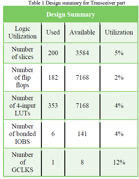
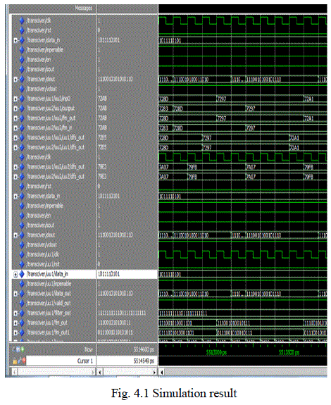
| Gaussian filter is implemented using distributed algorithm in transmitter part, acts as a lowpass filter to avoid interference to other channel which provides multiplierless structure, hence occupies less resources on FPGA, by using Xilinx configurable logic block (CLB) look-up table architecture. DFS architecture is used to perform modulation & demodulation in communication system. Table 1 shows the resources utilization and Fig. 4.1 shows the simulation result of the whole communication system. |
 |
 |
ADVANTAGES |
| Spectral efficiency and no interference of signals is achieved because of Gaussian filter. Distributed algorithm & DFSâÃâ¬ÃŸs multiplier less structure architecture gives less code complexity, low power consumption and area efficiency can be achieved. |
CONCLUSION |
| To avoid interference of signals Gaussian filter is implemented using DA before modulation, which performs multiplication using look-up table based method, uses less operations and hence reduced delay, area optimization & high power efficiency is achieved. |
References |
|