Keywords
|
| Adaptive FIR filter, Distributed Arithmetic, carry-save accumulation, Adaptive LMS algorithm, offset Binary Coding. |
INTRODUCTION
|
| Off late, adaptive FIR filters are part of almost all DSP applications. Its simplicity and better convergence performance makes it a widely used adaptive filter. The weights of the tapped delay-line finite impulse response (FIR) filter are updated using the well known Widrow-Hoff least mean square (LMS) algorithm [1]. A long critical path on the forward path of FIR filter design will be resulted in the direct form realization. This is because of the inner product computation to obtain the filter product. So, if the input signal has the high sampling rate, we have to reduce the critical path of the structure so that the critical path could not exceed the sampling period. |
| In recent days, multiplier less algorithms based on distributed arithmetic (DA) techniques has gained much popularity. Such a structure will have more advantages like high throughput because of its regularity, cost and area efficiency. Allred et al [3] proposed hardware –efficient DA-based design which uses two different lookup tables (LUTs) for updating weight and filter coefficients. Song Yoon Park and Promod kumar proposed an architecture [4] for implementing adaptive FIR filters. But the architecture is complex for higher order filters. |
| So, here a less-complex architecture is proposed for implementing adaptive FIR filter. Such a simpler design is possible with the help of “Offset Binary Coding”. Offset binary coding is a digital coding scheme. In this coding scheme, minimum negative value is represented by all zeros and the maximum positive value is represented by all-ones. This coding scheme has no standards, but the offset K=2^ (n-1) is most often used for an n-bit binary word. Here the “zero” value is represented by all zeros except the most significant bit, which is similar to two’s complement notation except the most significant bit is inverted. |
| Offset binary coding finds more applications in Digital Signal Processing (DSP) [5]. The basic units of DSP chips are analog to digital (A/D) and digital to analog (D/A) converters. These are unipolar so cannot process bipolar signals. For that biasing the analog signals with a DC offset is needed. The result is in offset binary format. Offset binary format cannot be handled directly by most of the standard computer CPU chips. They typically require some data conversion techniques to process offset binary. But without requiring any data conversion DSP chips can handle offset binary. Just by inverting the most significant bit offset binary can be converted into two’s complement form. |
II. RELATED WORK
|
| Basant K.Mohanty and Pramod Kumar Meher [6] proposed DA based design which uses an LUT- sharing technique for the computation of filter outputs and weight increment in terms of BLMS algorithm. Besides it offers significant saving of adders which constitute major component of DA based structures. Both convolution and correlation are performed using a common LUT for the computation of filter outputs and weight increments respectively. Also a novel LUT updating scheme is suggested to update the LUT contents for DA based BLMS adaptive FIR filter. Where one set of LUTs out of M sets need to be modified once in every M iterations, N=ML, N is the filter length and L is the input block size. |
| The numbers of adders required by the proposed structure in this paper does not increase linearly with N. It involves less number of LUT access per output than existing. This is the major advantage of the design for the reduction for ADP and EPO when implemented for larger order Adaptive FIR filters. Comparing with the best of the existing designs this involves nearly L/6 times more adders and L times more LUT words and offers nearly L times throughput. It requires nearly 25% more flip-flops irrespective of the block size. |
| In case of pipelined designs, the feedback-error e(n) become available after certain number of cycles, called the “adaptation-delay”. The pipelined architectures therefore use the delayed error e(n- m) for updating the current weight instead of the recent-most error, where m is the adaptation delay |
| P. K. Meher and S. Y. Park [7] proposed an efficient architecture for high-speed DA based adaptive filter with very low adaptation-delay. As the previous papers consisting of single LUT will not support the high sampling rate, because the number of cycles required for the each new sample update is more this problem is encountered in this paper. This is further improved in the present paper. The clock period required for this design is less compared to the proposed design. |
| R. Guo and L. S. DeBrunner [8] proposed an hardware efficient adaptive filter architecture and presents the single LUT for the both input and weight update is used. But the number of cycles required for the each new sample adaption takes more number of cycles. This increases the power dissipation and decreases the throughput rate. |
| K.Jebin roy, and R.Ramy [9] proposed an adaptive FIR filter structure using distributed arithmetic (DA) for area efficient design is implemented. High throughput is drastically enriched by parallel (LUTs) update and equivalent implementation of filtering and weight-update operations. The proposed carry save accumulation using 10 transistor full adder schemes of signed partial inner products for the computation of the filter output and also modified in weight increment block. By this way it utilizes low area, low power consumption and the throughput of the filter rates increases irrespective of the filter length. |
III. CONCEPT OF ADAPTIVE LMS ALGORITHM
|
| The LMS algorithm computes both the filter output and an error value during each cycle. Usually the difference between current filter output and desired responses is termed as error value. Then the filter coefficients are updated with an estimated error value in every training cycle. The filter coefficients are updated during the nth iteration according to the following equations: |
 (1) (1) |
| Error signal is given as |
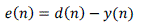 (2) (2) |
| Output signal of the adaptive filter is |
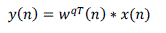 (3) (3) |
| Where ??(??) is the filter coefficients vector, and ??(??) is the filter input vector, ??(??) is the desired response, ?? is the convergence factor. The feedback error ??(??) will be available after certain number of cycles in the case of pipelined designs. This is called ‘Adaptation Delay’. So, the delayed error ??(?? − ??) is used for updating the current weight in pipelined structure instead of the most recent error, the parameter ‘m’ is the adaptation delay. The equation that governs such weight update in an adaptive filter using LMS algorithm is given by |
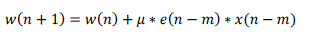 (4) (4) |
| Here x(n) is filter input vector and w(n) is weight vector. |
IV. DA-BASED APPROACH FOR INNER-PRODUCT COMPUTATON
|
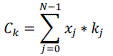
| In the LMS adaptive filter, inner-product computations of the critical path in each cycle are performed by using the following expression. |
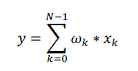 (5) (5) |
| Where ???? and ???? form the N-point vectors corresponding to the current weights and the most recent N-1 input values respectively for 0 ≤ k ≤ N-1. Let L be the bit width of the weight and each component of the weight vector in its 2’s complement representation is expressed as |
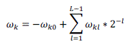 (6) (6) |
| Where ??????denotes the lth bit of ????. Now eq.(5) can be written as |
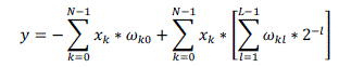 (7) (7) |
| In the above equation by altering the summations order of k and l indices it can be converted to sum-of-products form. |
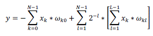 (8) (8) |
| From the above equation the inner-product can be calculated as |
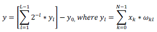 (9) (9) |
| The partial sum ???? for l = 0,1,….,L-1 will have 2?? possible values. The inner-product of above eq. will be calculated for L cycles of shift accumulation; thereafter for L number of bit slices {??????} where 0 ≤ l ≤ L-1 corresponding LUTread operations will be performed as shown in fig.1. and the shift accumulation is performed using carry-save accumulator as it involves significant critical path. |
| In carry-save accumulation the weight vector ?? bit slices are given one after the next in the order LSB to MSB. In the case of MSB slices the accumulation of output in its 2’s complement form is needed. Therefore, all the bits of LUT output are passed through the XOR gates with a sign-control input as the result is represented in two’s complement format. The output will be set to one if the appeared address is MSB slice. |
| Thus the XOR gates produce the LUT output of MSB slice in one’s complement form without affecting the output of other bit slices. At last both the outputs of XOR gate (i.e. sum and carry words ) resulted after L number of clock cycles have been added by the final adder and the input carry to the final adder is set to one to account for performing 2’s complement operation of the LUT output of the MSB slice. |
| The equation that gives data in Kth LUT location is as |
 (10) (10) |
| In the above expression ???? is the (j+1)th bit of N-bit binary representation of integer k for 0 ≤ k ≤ 2??-1. Here ???? for 0 ≤ k ≤ 2??-1 can be precomputed and stored in RAM-based LUT of 2?? words. However, only (2??-1) registers are stored in LUT instead of storing 2?? words. |
| V.EXISTING DA-BASED ADAPTIVE FILTER STRUCTURE |
| For our convenience we can decompose the computations of the large ordered adaptive filters into small adaptive filtering block. This makes the job of computing inner product which is the most important task in DA- based implementation of adaptive filters easier as the inner product computation of long vectors requires a very large LUT(3). The existing DA-based LMS adaptive filter design requires 16 delay element DA-table structure. The 4th order adaptive filter (N=4) implementation involves a four-point inner product block, weight increment block and the circuit for generating error ‘e’, and a control word generator that generates the control word ‘t’ for the barrel shifters as shown in fig 2. |
| But the same structure can be implemented with the help of 8-delay elements. Since with the help of basic elements x(n), x(n-1), x(n-2), x(n-3) the remaining structure can be implemented. It can be achieved with the help of Offset Binary Coding (OBC). |
VI.PROPOSED OFFSET BINARY CODING BASED ADAPTIVE FILTER DESIGN
|
| In the proposed approach, for the implementation of DA-based adaptive filter, we make use of the DA-table structure that makes use of the 8 delay elements. Hence by using the proposed structure, we can reduce the original DA-table structure by two times, which increases the area efficiency of the design twice. The proposed structure for the DA-table which makes use of eight delay elements is shown in the fig.3. |
| The proposed structure for 4th order adaptive filter (N=4) is shown in the fig 2. Generally, it consists of a four-point inner product block, a weight increment block and the circuit for generating error ‘e’, and a control word generator that generates the control word ‘t’ for the barrel shifters. |
| The four point inner product block which was shown in fig.4., consists of a DA-table which has an array of 15 registers. It is capable of storing the partial inner products ‘y’, for 0 < l ≤ 15 and a 16:1 multiplexer is used to select one of those registers at any particular instants. Weights A= {w?, w?, w? ,w?} for 0 ≤ l ≤ L-1 are fed to the multiplexer as control bits in the LSB-MSB order. The output of the MUX is then fed to the carry-save accumulation block. After L clock cycles, the carry-save accumulation block accumulates all the partial inner products and generates a sum word and a carry word of size L+2 bit length each. |
| The sum word is shifted right by one position right and added to the carry to generate the filter output y(n-1) which is then subtracted from the desired signal d(n) to obtain the error e(n). After that the sign-magnitude separator is used to separate the sign bit and magnitude bits from the obtained error |
| The magnitude bits are used by the control word generator to generate the control word ‘t’ for the barrel shifter. The logic used for the generation of control word ‘t’ for barrel shifter is shown in the fig. 4. |
| The convergence factor ‘μ’ is taken as 1/N. Generally, we can take μ as 2???? /N, where ‘i’ is a small integer.The weight increment unit for N=4 consist of four barrel shifters and four adder/subtractor cells. The structure of weight increment cell is shown in fig. 6. |
| In general Barrel Shifter is the most helpful unit in Digital Signal Processing blocks. Mostly it is used in multiplication and division operations. It performs multiplication just by right shifting the data in registers by required number of times |
| That means to multiply the data by 2 times, the data is shifted right by one position. Similarly division can be performed by left shifting the data as per requirement. Thus the barrel shifter reduces the complexity of operations there by area optimization has been achieved too. With these advantages barrel shifter has more importance in DSP chips |
| The above figures fig.5 and fig.4 shows the structure for a general four point inner product block and the logic used for the generation of control word for the barrel shifter respectively. |
| Here the barrel shifter shifts the input values ???? where k=0,1,….N-1 by defined number of locations. Barrel shifter yields the number of increments to be added or subtracted from the present weights. The sign bit from the signmagnitude separator is used as the control for adder/subtractor cells such that depending on the value of the sign bit whether it is zero or one, the barrel shifter output is respectively added or subtracted from the content of the weight corresponding current value in register |
| Thus the fourth order filter implementation is done successfully with 8-DA table structure. It reduces the complexity as the basic terms like x(n), x(n-1), x(n-2), x(n-3) are more enough to generate all the other terms. So higher order filters can also be easily implemented in hardware as this design achieves low-complexity. |
| The above fig.6 shows the structure of the weight increment block which takes the input from the control word generator |
VII. FURTHER IMPROVEMENT IN THE FILTER STRUCTURE USING OFFSET BINARY CODING
|
| By using Offset Binary coding, we can further improve the filter structure. The DA-table can be further reduced to 4- delay element structure with the help of Offset Binary coding. From the previous DA-table figures, we could observe that the entire structure can be built with the four basic and unique elements i.e. x(n),x(n-1),x(n-2),x(n-3). Hence, with the help of OBC, we can achieve same DA-table operation with only 4 delay elements. |
| Such a DA-table structure with 4 delay elements is shown in the above fig.7. By incorporating such a DAtable made up of 4 delay elements in the adaptive FIR filter structure improves its area efficiency considerably. |
A.HIGHER ORDER FILTER IMPLEMENTATION
|
| The structure of higher order filter of size N=16 is shown in fig 8. The design involves four sets of inner product blocks and weight increment blocks. All the blocks are connected in a proper manner in order to give a desired result. |
| The four 4-point inner product blocks and weight increment blocks all together is known as 16-bit data computing block as this sub block computes 16-bit sum and carry words. These are used in further computations. As in the case of fourth order filter implementation, here also the L+2 bit sums and carry are produced by the four inner product blocks. And these will be added by using two binary adder trees. The output of four 4-point inner-product inner blocks i.e. sum words are added with four carry-in bits. Since the carry words are of double the weight compared to the sum words, two carry-in bits are set as input carry at the first level binary adder tree of carry words, which is equivalent to inclusion of four carry-in bits to the sum words. Sign magnitude separator is used to separate sign bits and magnitude bits from the calculated error as in the case of smaller order filter designs. Outputs of sign-magnitude separator and control word generator are fed commonly to all the weight increment blocks. The logic used for control word generator is also same as that of previous logic. Further, the filtering process is same as that of the 4th order adaptive FIR filter except that the process is performed on 16-bit data instead of 4-bit data. |
| Similarly, the structure can be extended to 32-bit filter implementation. For that purpose two 16-bit data computing blocks which are mentioned earlier have been used. The structure of 32-bit filter is shown in the fig.9. Just by performing the binary addition of 16-bit sum and carry of the two 16-bit data computing blocks, the filter of length N=32 can be realized. The connections between the blocks must be given properly for achieving better results. |
| The above table presents the simulation results of the existing and proposed designs. The data proves that by employing the proposed technique, we could decrease the hardware complexity of the adaptive filter design considerably. We have coded the proposed & existing designs in VHDL and synthesized by Xilinx ISE Design tool 13.2 using a 95-nm CMOS library for filter length N = 16 and N = 32 to find the area, time, and power capabilities. The FPGA used is Spartan 3E, device used is XC3S500E, package used is FG320 and speed is -4. In the above table, we have shown the synthesis results in terms of no. of slices, no. of slice flip flops and the no. of 4-input LUTs used. From the synthesis reports, we find that the power consumption was 81 milli watts and remains almost constant even though the order of the adaptive filter is increased to N = 16 and N = 32. |
IX.CONCLUSION
|
| Low-complexity design implementations have greater importance in efficient hardware implementations. In this brief architecture for the implementation of adaptive FIR filters is proposed. This design achieved low-complexity compared to existing DA-based implementations. |
Figures at a glance
|
 |
 |
 |
 |
 |
| Figure 1 |
Figure 2 |
Figure 3 |
Figure 4 |
Figure 5 |
|
 |
 |
 |
 |
| Figure 6 |
Figure 7 |
Figure 8 |
Figure 9 |
|
References
|
- S. Haykin and B. Widrow, Least-Mean-Square Adaptive Filters. Hoboken, NJ, USA: Wiley, 2003.
- S. A. White, ?Applications of the distributed arithmetic to digital signal processing: A tutorial review,? IEEE ASSP Mag., vol. 6, no. 3, pp. 4?19, Jul. 1989.
- D. J. Allred, H. Yoo, V. Krishnan, W. Huang, and D. V. Anderson, ?LMS adaptive filters using distributed arithmetic for high throughput,? IEEE Trans. Circuits Syst.I, Reg. Papers, vol. 52, no. 7, pp. 1327?1337, Jul. 2005.
- Sang Yoon Park and Promod Kumar Meher, ?Low- power, High-Throughput, and Low-area Adaptive FIR Filter Based on Distributed Arithmetic,? IEEE Trans. OnCircuits and Systems-II, Express Briefs, Vol.60, no.6, pp.346-350, June 2013.
- W. Huang and D.V. Anderson, ?Modified Sliding-Block Distributed Arithmetic with Offset Binary Coding for Adaptive Filters,? Journal of Signal Processing Systems,April 13, 2010.
- Basant K.Mohanty and Pramod Kumar Meher ?A high performance energy efficient architecture for FIR adaptive filter based on new distributed arithmeticformulation of block LMS algorithm? IEEE transactions on signal processing,vol.61,no.4,pp.921-931,feb.2013.
- P. K. Meher and S. Y. Park, ?High-throughput pipelined realization of adaptive FIR filter based on distributed arithmetic,? in IFIP/IEEE International Conference onVery Large Scale Integration, Oct. 2011. pp. 428?433.
- R. Guo and L. S. DeBrunner, ?A novel adaptive filter implementation scheme using distributed arithmetic,? in Asilomar Conference on Signals, Systems andComputers, Nov. 2011, pp. 160?164.
- K.Jebin roy, and R.Ramy ?Low power and low area adaptive FIR filter based on distributed arithmetic and LMS algorithm? International Journal of Scientific andResearch Publications, Volume 4, Issue 3, March 2014
|