Keywords
|
| Adiabatic circuits,Low power VLSI,CPAL,T flip flop |
INTRODUCTION
|
| Increasing demand to improve the portable system performance has fuelled the necessity of low-power design techniques. Longer battery operational life has become a major design goal in low-power VLSI system. Adiabatic switching technique based on energy-recovery principle was proposed to reduce power dissipation in digital circuit. Conventional CMOS circuits are driven by constant voltage supply and a significant amount of battery power is wasted as thermal energy in resistive circuit elements. This wastage of energy occurs due to charging and discharging of the load capacitor through transistors operated in linear regions and equals to CV2 DD f. In order to minimize this energy loss, innovative energy-recovery adiabatic circuits were proposed. These circuits use power-clock voltage in the form of a ramp or sinusoidal signal. The power clock supply has the two fold role and is used as power supply signal and clock signal. This avoids the need of two separate sources. |
II. ADIABATIC LOGIC
|
2.1 Adiabatic Logic
|
| Fig.1.1. shows the general circuit topology of an adiabatic counterpart. To convert a conventional CMOS logic gate into an adiabatic gate, the pull-up and pull-down networks must be replaced with complementary transmission-gate networks. The T-gate network implementing the pull-up function is used to drive the true output of the adiabatic gate, while the T-gate network implementing the pull-down function drives the complementary output node. Note the all inputs should also be available in complementary form. Both networks in the adiabatic logic circuit are used to chargeup as well as charge-down the output capacitances, which ensure that the energy stored at the output node can be retrieved by the power supply, at the end of each cycle. To allow adiabatic operation, the DC voltage source of the original circuit must be replaced by a pulsed-power supply with ramped voltage output. Note that the circuit modifications which are necessary to convert a conventional CMOS logic circuit into an adiabatic logic circuit increase the device count by a factor of two. Also, the reduction of energy dissipation comes at the cost of slower switching speed, which is the ultimate trade-off in all adiabatic methods. |
2.2 Adiabatic Switching
|
| A typical adiabatic switching circuit is as shown in Fig.1.3. Here, the load capacitance is charged by a constant current source, which corresponds to a linear voltage ramp. The main difference between the conventional CMOS circuits and the adiabatic circuits is that in adiabatic circuit the load capacitor is charged by a constant current source while in |
| Conventional CMOS circuit, it is charged by a constant voltage source. In the Fig.1.3. let R be the on-state resistance of |
| pull-up network of the circuit. |
| Assuming Vc(t)=0 at t=0 |
| Vc(t) =(1/C)Isourcet |
| Where, |
| Isource =C (Vc(t)/t) |
| Energy dissipated in the resistor R from t=0 to t=T can be found as |
| Ediss=R∫ Isource 2dt |
| = Isource 2RT |
| =(RC/T)C Vc 2(t) |
| From this equation it is observed that; |
| (1) If charging time is greater than 2RC then the dissipated energy is smaller thanthat for conventional CMOS circuit. |
| (2) Dissipated energy is inversely proportional to T, which means that dissipated energy can be made arbitrarily smaller by increasing the charging time |
| (3) Dissipated energy is proportional to R in contrast to conventional CMOS case where in dissipated energy depends on load capacitor and voltage swing. |
| (4) As charging resistance decreases, the energy dissipated decreases. |
| Fig.1.2 depicts the charge flow in adiabatic circuit. Pull-up circuit drives the true output of the adiabatic gate while pull-down circuit drives the complementary output node. Both the networks in adiabatic charge up as well as charge down the output capacitor. At the end of the cycle, the energy flows back into the power supply. The important component in this circuit is the pulsed power supply with ramped voltage instead of a DC supply in conventional logic |
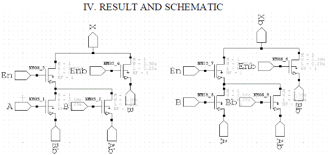
| The CPAL family is the best solution for Sequential Adiabatic circuit design which consists of two main circuits, one is the logic function circuit and other is the load driven circuit. Proper choice of logic function circuit generates any logical identity with CPAL family. |
3.1 Implementation of CPAL Gates
|
| The basic structure of the CPAL buffer is shown in Fig. 3.1. It is composed of two main parts: the logic function circuit and the load driven circuit. The logic circuit consists off our NMOS transistors (N5–N8) with complementary pass transistor logic (CPL) function block. The load driven circuit consists of a pair of transmission gates (N1, P1 and N2, P2).The clamp transistors (N3 and N4) ensure stable operation by preventing from floating of the output nodes. Cascaded CPAL gates are driven by the two-phase non-overlap power-clocks. |
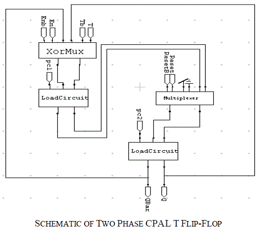
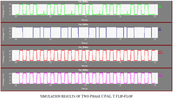
3.2 Two phase CPAL T flip-flop
|
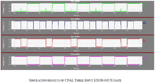
| Two phase CPAL T flip-flop is implemented combining CPAL 2:1 MUX with CPAL EXOR-MUX gate as shown in the Fig.3.10. The T flip-flop with reset and enable terminals based on two-phase CPAL circuits are shown .Because pre-settable flip-flops are more universal and suitable for the design of adiabatic sequential circuits, a reset line is added for the adiabatic T flip-flops by using a multiplexer. When Reset is logic ‘1’, the output Q is set to ‘0’. If Reset is ‘0’, the function of the multiplexer is the same as a CPAL buffer. An enable terminal (EN) has also been added for the T flip-flop. Assume that the present state of flip-flops is Q. Then, when EN is logic ‘1’, next state Q+of the T flip-flop can be written as Q+T Q . If EN is ‘0’, the next state is Q+= Q.Complex sequential circuits can also be realized |
 |
 |
 |
 |
V. CONCLUSION
|
| The implementations of adiabatic flip-flops and sequential circuits are described in this paper. The flip-flops are realized with the two-phase CPAL (complementary Pass transistor adiabatic logic) circuits The two-phase non-overlap power-clock generator is used to supply the CPAL sequential circuits, which is realized by using a simple converter and single-phase sinusoidal power-clock. A power-gating scheme for the adiabatic sequential circuits can be proposed. The adiabatic sequential circuits with the power-gating scheme attain large energy savings over a wide range of frequencies, as compared with conventional CMOS circuits. |
Figures at a glance
|
 |
 |
 |
 |
| Figure 1 |
Figure 2 |
Figure 3 |
Figure 4 |
|
| |
References
|
- Dong Zhou, Jianping Hu, and Ling Wang, “The Implementations of Adiabatic Flip-Flops and Sequential Circuits with Power-GatingSchemes”, International Conference of Circuits and Systems ,MWSCA ,IEEE 2008.
- P. D. Khandekar, and S. Subbaraman, “Low Power Inverter and Barrel Shifter Design Using Adiabatic Principal”, International Conference Of Advances in Computational Sciences and Technology , ISSN 0973-6107 Volume 3 Number 1 pp. 57–65 ,2010
- Weiqiang Zhang, Yu Zhang, Shi Xuhua, and Jianping Hu , “ Leakage Reduction of Power- Gating Sequential Circuits Based on Complementary Pass-transistor Adiabatic Logic Circuits ”, International Conference on Innovative Computing and Communication , 2010.
- Jianping Hu and Jinghong Fu, “Leakage Dissipation Reduction of Single-Phase Power Gating Adiabatic Sequential Circuits Using MTCMOS ”,International Conference on Electrical and Control Engineering , 2009.
- Haiyan Ni and Jianping Hu, “Single-Phase Adiabatic Flip-Flops and Sequential Circuits with Power-Gating Scheme”,International conferenceof ASICON , 2009 .
- Dong Zhou, Jianping Hu, and Ling Wang, "Adiabatic Flip-Flops for Power-Down Applications," IEEEISIC'07, pp. 493-496, 2007.
- J. P. Hu, T. F. Xu, Y. S. Xia, “Low-power adiabatic sequential circuit with complementary pass-transistor logic,” IEEE MWSCAS’05, pp.1398- 1401, USA, August 7-10, 2005.
- Y. Moon, and D. K. Jeong, “An efficient charge recovery logic circuit,” IEEE J.of Solid-State Circuits,vol.31(4), 1996.
- P D Khandekar, S Subbaraman, Manish Patil, “Low Power Digital Design Using Energy-Recovery Adiabatic Logic,” International Journal of Engineering Research and Industrial Applications, Vol. 1, No. III, pp 199-208,2009
|