Finite Field arithmetic is becoming increasingly a very prominent solution for calculations in many applications. Galois Field arithmetic forms the basis of BCH, Reed-Solomon and other erasure coding techniques to protect storage systems from failures. Most implementations of Galois Field arithmetic rely on multiplication tables or discrete logarithms to perform this operation. Software-based Galois field implementations are used in the reliability and security components of many storage systems. Unfortunately, multiplication and division operations over Galois fields are expensive, compared to the addition. To accelerate multiplication and division, most software Galois field implementations use pre-computed look-up tables, accepting the memory overhead associated with optimizing these operations. However, the amount of available memory constrains the size of a Galois field and leads to inconsistent performance across architectures. Typical arithmetic unit includes an adder or subtracter, multiplier and divider. Addition operation is done with one n-bit XOR operation, for multiplication operation LSB first multiplying method is used and Fermat’s little theorem for multiplicative inverse operation. These operations are implemented on FPGA Virtex v.5 kit & simulated using Verilog on Xilinx 14.2 ISim simulator. Arithmetic unit architecture is measuredin terms of %age of device utilized and time delay.
Keywords |
| Finite field, BCH, Galois field, Inversion, Adder, Multiplier, Divider |
INTRODUCTION |
| Finite fields are algebraic structures that are used in error-correcting coding, cryptography and digital signal
processing. Many of the most important mathematical results of finite fields date back to the nineteenth century, but it
was not until the introduction of error-correcting codes in the 1950s that they came to any practical use |
| Arithmetic in a finite field is different from standard integer arithmetic. There are a limited number of elements in
the finite field; all operations performed in the finite field result in an element within that field. Finite fields are used in
a variety of applications, including in classical coding theory in linear block codes such as BCH codes and Reed
Solomon error correction and in cryptography algorithms such as the Rijndael encryption algorithm |
| Wireless broadband radio transmissions and computer hard drive storage are applications where the error
correction is necessary, and where the demands on the coding and decoding speed are growing. If such systems are to
work under more and more extreme conditions, effective error-correcting codes must be used, which in turn means that
there is a need for faster arithmetic operation. |
| There are number of ways of performing finite field arithmetic. One method is the use of software algorithms that
perform the computations in a processor. That is flexible method, since the processor can normally be programmed for
any finite field or field representation. A large drawback is that the computations are slow, since the processor is
normally not optimally designed for finite field arithmetic |
| Significantly better performance can be achieved if these computations are done in hardware. There are many
optimized implementations of specific coding schemes with fixed field representations. That means they can perform
coding and decoding very efficiently, but they are also limited to only one single application |
| With these facts in mind it would obviously be interesting to find a solution that combines the speed of hardware,
and the flexibility of software. One way of doing this is by designing a hardware arithmetic unit that can be used as an
external hardware unit or included as an integrated part while designing the signal processor. This arithmetic unit can
be used in the communication with many sources that use different coding schemes |
II. RELATED WORK |
| There have been lot of work being done on finite field arithmetic operation. There are few examples of finite field
processors, but most of these have been designed for cryptographic applications which have different requirements.
Two examples are provided by Hasan and Wassal [2] and Kim and Lee [3]. The idea of designing a finite field
arithmetic unit for error-correcting coding seems to be interesting one |
| The hardware architectures for multiplication and inversion have been developed by a number of people over many
years. Finite field arithmetic is a well-studied branch in mathematics, and hardware implementations have been known
for many years. A number of early proposals can be found in Berlekamp [4]. The first systolic architectures were
proposed in the 80’s and have been further developed since. |
| Some examples of implementations of bit-serial systolic arrays for multiplications are given by Wang and Lin [5],
Tsai and Wang [6]. Digital-serial systolic multipliers have been proposed by Kim, Han and Hong [7] and Guo and
Wang [8]. |
III. PROPOSED WORK |
| The purpose of this paper is to provide with an elementary knowledge of algebra that will aid in the understanding
of the material in the following topics. The treatment is basically descriptive and no attempt to made mathematically
rigorous. For any positive integer m, it is possible to extend the prime field GF(p) to a field of pm elements, which is
called an extension field of GF(p) and is denoted by GF(pm ). A large portion of algebraic coding theory, code
construction, and decoding is built around finite fields. |
| The mathematical properties within which BCH codes and RS codes are definedalso represents Galois field. The
mathematical operations like Additions, Subtractions, Multiplications and Divisions are performed using Finite field
theory. The most basic axioms of the finite field are: |
| 1. All the elements in the field forms an Abelian group with additional operator “+”. |
| 2. The non-zero elements in the field forms group with multiplication operator “.”. |
| 3. Multiplications by any non –zero elements is an automorphism of the Additive group. |
| A. GF (24) |
| The main reason of constructing a GF (2m) is that they do not have both 0 and 1 as their roots. This section is
provided with a detailed explanation of Galois field (24). Consider the below equation |
 |
| From the above equation, it is clear that, neither 0 nor 1 is the root for of the equation. So, we can say that the 4th order
root of equation (1) lies outside of the GF (24) field. By assuming α as one of the root of the equation, P(α) should be
equal to zero. This can be explained by below equation |
 |
| The above equation (2) can be used to generate GF (24). Rearranging the above equation gives, |
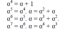 |
| The higher order field elements can be generated similarly by multiplying α to its previous power. The fifteenth power
of α can be calculate as below: |
| α15 = α14. α = 1. |
| Here, the simplification of the fifteenth order gives 1, which is an existing element so; further powers of α will always
give the existing elements. Therefore the field GF (24) has the following 16 elements: |
| 0, 1, α, α2, α3, α4, α5, α6, α7, α8, α9, α10, α11, α12, α13, α14 |
B. Galois Field Arithmetic Unit – Design and Architecture |
| Arithmetic Unit refers to the unit which performs the mathematical operations on a given field. This topic
explains about the design and architecture of Arithmetic Unit based on Galois Field elements and its implementation on
FPGA (Virtex v.5). The computations performed over Arithmetic Unit are required for encoding and decoding of
various error correcting codes such as BCH and RS codes which can be programmed easily on general purpose
computer. |
➢ Galois Field Adder |
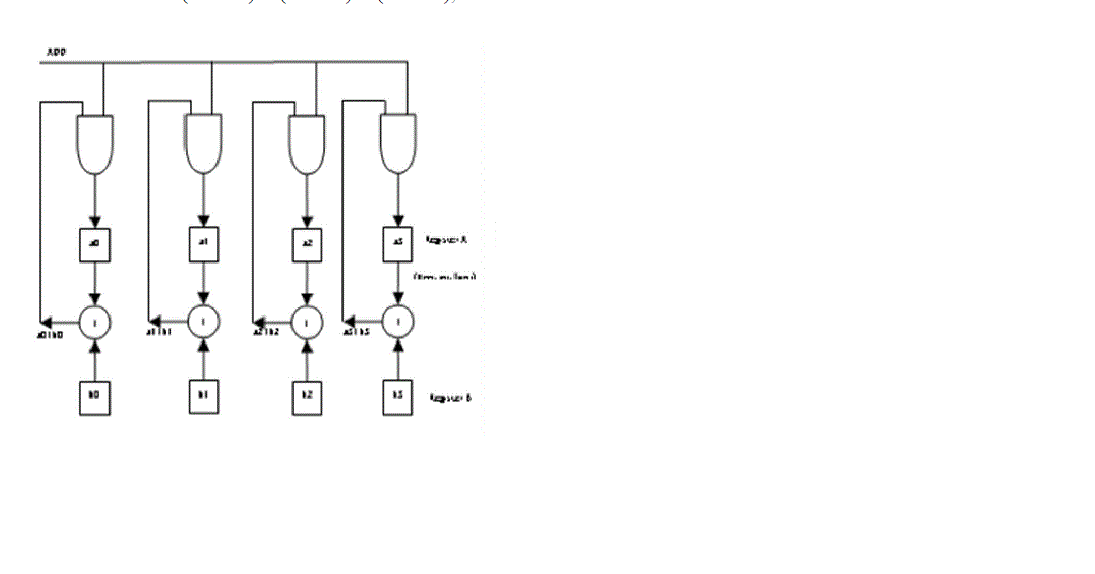
| Two field elements can be added with the circuit shown in Fig.2. First, the vector representation of the two
elements to be added is loaded into registers A and B. Their vector sum then appears at the inputs of register A. When
register A is pulsed (or clocked), the sum is loaded into register A (register A serves as an accumulator).For example, if
we want to add α7 and α13 of GF (24). We know that their vector representation are (1 1 0 1) and (1 0 1 1), respectively.
Their vector sum is (1 1 0 1) + (1 0 1 1) = (0 1 1 0), which is the vector representation of α5. |
➢ Galois Field Multiplier |
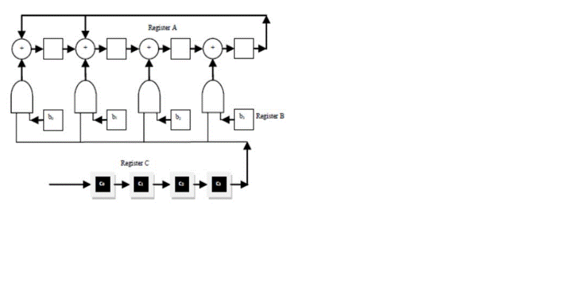
| Next, we consider multiplying two arbitrary field elements as in fig.3. Again, we use GF (24) for illustration.
Let β and γ be two elements in GF (24). Express these two elements in polynomial form: |
 |
| Then the product βγ can be expressed in the following form: |
 |
| This product can be carried out with the following steps: |
| 1. Multiply c3β by α and add the product to c2β. |
| 2. Multiply (c3β)α + c2β by α and add the product to c1β. |
| 3. Multiply ((c3β)α + c2β)α + c1β by α and add the product to c0β. |
➢ Galois Field Divider |
| The arithmetic operation of divisor over GF (2m) can be performed by first forming the multiplicative inverse
of the divisor β and then multiplying this inverse β-1 by the dividend, thus forming the quotient. The multiplicative
inverse of β can be found by using the fact β(2^m-1)=1. Thus, |
| β-1= β(2^m-2) (3) |
IV. HARDWARE IMPLEMENTATION &PSEUDO CODE |
| In this section, the design of arithmetic unit is implemented on Virtex v.5. Virtex-5 devices are offered
exclusively in high performance flip-chip BGA packages that are optimally designed for improved signal integrity and
jitter. Package inductance is minimized as a result of optimal placement and even distribution as well as an increased
number of Power and GND pins. The Xilinx XUPV5-LX110T is a versatile general purpose development board powered by the Virtex®-5 FPGA. It is a feature-rich general purpose evaluation and development platform, includes
on-board memory and industry standard connectivity interfaces, and delivers a versatile development platform for
embedded applications. |
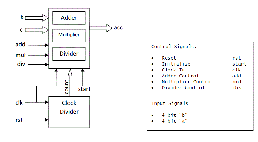
| Figure 2 shows the block diagram of an Arithmetic Unit. It consists of three major blocks namely Adder,
Multiplier and Divider along with the clock divider used for delaying the output. Each block has its own control signal,
which when triggered, does the respective operation. Below pseudo code shows the flow of signal from input to output
through different stages of Arithmetic Unit. |
Pseudo code: |
| Step 1. Initialize the inputs ‘b’ and ‘c’, control signals ‘start’, ‘add’, ‘mul’ and ‘div’, and the clock signal
‘clk’. |
| Step 2. If start = 0 |
| a. If add = 1, perform the addition operation. |
| b. If mul = 1, perform the multiplication operation. |
| c. If div = 1, perform the division operation. |
| Step 3. Give the respective output at ‘a’ |
| Step 4. If start = 1, give the default output as 0 |
V. SIMULATION RESULTS |
| In this section, simulation and synthesis results of arithmetic unit is discussed. The unit has been simulated
using Xilinx 14.2 ISim simulator and functionality is verified. Synthesis was carried out using RTL schematic viewer.
Moreover the device utilization is also summarized for Virtex v.5 kit. |
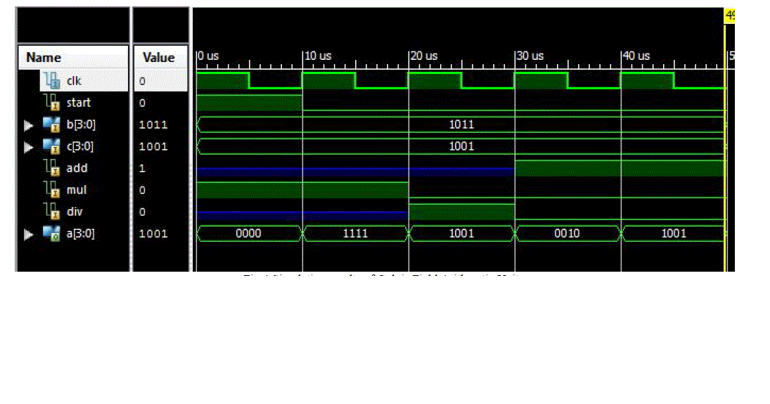
| Fig. 4 shows the simulation result of Galois Field Arithmetic Unit on ISim. Here, in this result we have taken a pulse
clock of period 10us. At first clock, the designed unit is reset which gives the output “0000”. The output of arithmetic
unit is shown in table 2 as per the pulse clock,input and control signal |
| Table 3 shows the hardware used for designing the arithmetic unit on FPGA. In FPGA viz. Virtex v.5, we have total
of 69120 slice registers and slice LUTs out of which only 31 registers and 62 LUTs are used. Aslice LUTs contains
block RAM, FFs and multiplexers. A collection of registers and flip-flop is referred to as configurable logic block
(CLB). Device used for design of arithmetic unit is much less compared to its availability. So, the complexity is very
less and operation is much faster. |
➢ Advanced HDL Synthesis Report:- |
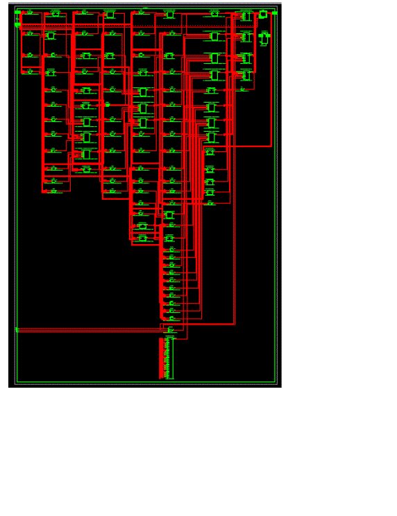
| Fig.5 shows the RTL schematic of Galois Field Arithmetic Unit on FPGA. It gives detailed explanation of how many
logic gates, Flip-flops, counter etc. used for design of architecture. Here a 27-bit up counter is used for clock division
so that the output is visible on LED of Virtex v.5. Timing summary gives the details of delay and maximum frequency
of operation of the arithmetic unit. Here maximum frequency is 381.876 MHz below which this device can be operated. |
| Macro Statistics |
| # Counters : 1 |
| 27-bit up counter : 1 |
| # Registers : 4 |
| Flip-Flops : 4 |
| # Xors : 34 |
| 1-bit xor2 : 18 |
| 1-bit xor3 : 4 |
| 1-bit xor4 : 4 |
| 1-bit xor5 : 8 |
➢ Timing Summary |
| Speed Grade : -2 |
| Minimum period : 2.619 |
| (Maximum Frequency: 381.876MHz) |
| Minimum input arrival time before clock:4.660ns |
| Maximum output required time after clock: 2.830ns |
VI. CONCLUSION |
| In this paper, we propose an efficient finite field arithmetic unit in binary finite field GF (24) which is used in
most of the encoding and decoding applications to compute arithmetic operations which are essential for error detection
and correction. This one would be efficient when compared to the other arithmetic units. |
| This paper covers the history of Galois field and mathematical properties associated with it. Design of
Arithmetic Unit is discussed here which performs mathematical operations like addition, multiplication and division.
Subtraction operation is not discussed because the subtraction operation is same as addition in case of Galois field
arithmetic. |
Tables at a glance |
|
|
| |
Figures at a glance |
 |
 |
 |
 |
 |
| Figure 1 |
Figure 2 |
Figure 3 |
Figure 4 |
Figure 5 |
|
| |
References |
- S. Lin, and D.J. Costello, Jr., âÃâ¬ÃÅError Control CodingâÃâ¬ÃÂ, Prentice-Hall, New Jersey, 1983.
- A.G.WassalM.A.Hasan. VLSI algorithms, architectures andimplementation of a versatile GF (2m). IEEE Transactions on computers, Vol. 49No.10, 2000.
- Dong-Ho Lee Ju-Hynn Kim. A compact finite field processor over GF(2m) for elliptic curve cryptography. IEEE, 2002.
- Elwyn R. Berlekamp. Algebraic Coding Theory, McGraw-Hill Book Company, 1968.
- Jung-Lung Lin Chin-Liang Wang. Systolic array implementation of multipliers for finite fields GF (2m). IEEE Transactions on Circuits andSystems, Vol. 38, No. 7, 1991.
- S.-K. Wang W.C. Tsai. Two systolic architectures for multiplication in GF (2m).IEEE Proc.-Comput. Digit.Tech. Vol. 147, No. 6, 2000.
- Chun Pyo Hong Chang Hoon Kim, Sang Duk Han. An efficient digit serial systolic multiplier for finite fields GF (2m). IEEE, 2001.
- C.-L. Wang J.-H.Guo. Digit-serial systolic multiplier for finite fields GF (2m) .IEEE Proc.-Comput. Digit.Tech. Vol. 145, No. 2, 1998.
|