This paper analyzes the parasitic effects in SAR ADCs. Which achieves a significant switching energy saving when compared with set-and-down and charge-recycling switching approaches. Successive approximation technique in ADC is well known logic, where in the presented design the linearity analysis of a Successive Approximation Registers (SAR) Analog-to-Digital Converter (ADC) with split DAC structure based on two switching methods: VCM -based switching, Switch to switchback process. The main motivation is to implement design of capacitor array DAC and achieve high speed with medium resolution using 45nm technology. The current SAR architecture has in built sample and hold circuit, so there is significant saving in chip area. The other advantage is matching of capacitor can be achieved better then resistor. Which is verified by behavioural Measurement results of power, speed, resolution, and linearity clearly show the benefits of using VCM-based switching? In the proposed design the SAR ADC is designed in switch to switchback process such a way that the control module completely control the splitting up of modules, and we planning to give an option to change the speed of operation using low level input bits. A dedicated multiplexer is designed for that purpose system.
Keywords |
| Linearity analysis, linearity calibration, resolution SAR ADCs, split DAC, VCM-based switching,
switch to switch back process. |
INTRODUCTION |
1.1 Selection of the right ADC architecture |
| The selection of the right architecture is a very crucial decision. The following fig.1 shows the common ADC
(Analog to Digital Converter) architectures, their applications, resolutions and sampling rates. Sigma Delta ADC
architectures are very useful for lower Sampling rate and higher resolution (approximately 12-24 bits). |
| The common applications for Sigma-delta ADC architecture are found in voice band, audio and industrial
Measurements. The Successive Approximation (SAR) architecture is very suitable for data acquisition; it has
resolutions ranging from 8bits to 18 bits and sampling rates ranging from 50 KHz to 50 MHz The most effective way to
create a Giga rate application with 8 to 16 bit resolution is the pipeline ADC architecture. |
1.2 SAR ADC Architecture |
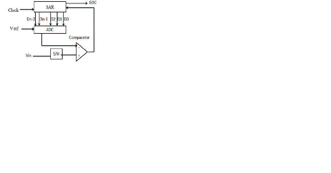
| The SAR architecture mainly uses the binary search algorithm. The SAR ADC consists of fewer blocks such as one
comparator, one DAC (Digital to Analog Converter) and one control logic.The algorithm is very similar to like
searching a number from telephone book. For example, to search a telephone number from telephone book, first, the
book is opened and the number may be located either in first half or in the second half of the book. Further, relevant
section is divided into half. This procedure can be followed until finding relevant number. The main advantage of SAR
ADC is good ratio of speed to power. |
| The SAR ADC has compact design compare to flash ADC, which makes SAR ADC inexpensive. The physical
limitation of SAR ADC is, it has one comparator throughout the entire conversation process. If there is any offset error
in the comparator, it will reflect on the all conversion bits. The other source is gain error in DAC. However, the static
parameter errors do not affect dynamic behaviour of SAR ADC. |
1.2.1 SAR Logic |
| SAR logic is purely a digital circuit, and it consists of three major blocks, |
| • Counter |
| • Bit register |
| • Data register |
| The counter provides timing control and switch control. For 8 bits conversion, seven DFFs (D flip-flops) are used. The
following table 1 explains which bit set to high during different phases of SAR operation. |
 |
II. EXISTING SYSTEM |
2.1 VCM Based Switching |
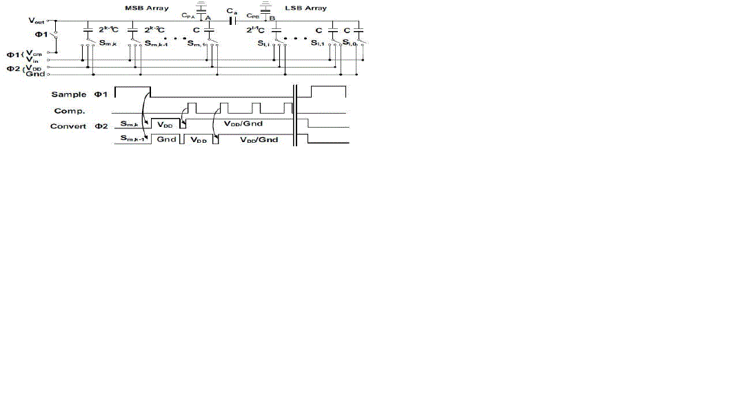
| The conventional binary weighted capacitor array has limitation for higher resolution due the larger capacitor ratio
from MSB capacitor to LSB capacitor. To eliminate this problem, one technique can be applied known as split
capacitor technique. For example, to achieve the 8bits resolution, the capacitor array can be spited as shown in
following fig.3. |
| The attenuation capacitor divides the LSB capacitor array and MSB capacitor array. Here, the ratio between LSB to
MSB capacitor (C to 8Cc) reduces drastically compare to the conventional binary weighted capacitor array. |
| The Vcm-based approach performs the MSB transition by connecting the differential arrays to Vcm. Thepower
dissipation is just derived from what isneeded to drive the bottom-plate parasitic of the capacitive arrays, while in the
conventional charge-redistribution where the necessary MSB “up” transition costs significant switching energy and
settling time. Moreover, as the MSB capacitor is notrequired anymore, it can be removed from the n-bit DAC array.
Therefore, the next n − 1 b estimation is done with an (n − 1) bit array instead of its n-bit counterpart, leading to half
capacitance reduction with respect to the conventional method. |
2.2 Sampling phase |
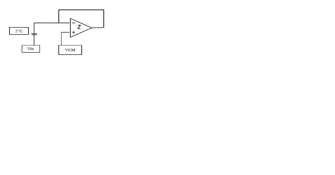
| During sampling phase bottom plates of capacitor array are connected to Vin as shown in fig.4. The reset switch still on
hence the top plate is on VCM; and voltage across capacitor array is Vin-VCM.During Charge transfer phase, bottom
plates of capacitor array are switched to VCM and top plates are floating as shown figure 7. In this phase, reset switch
is off. Hence, Voltage at top plate Vx During Charge transfer phase, bottom plates of capacitor array are switched to VCM and top plates are floating as
shown figure 7. In this phase, reset switch is off. Hence, Voltage at top plate Vx, which is as follows: |
2.4 Sample and Hold |
| In general, Sample and hold circuit (SHC) contains a switch and a capacitor. In the tracking mode, when the sampling
signal is high and the switch is connected, it tracks the analog input signal. Then, it holds the value when the Sampling
signal turns to low in the hold mode. In this case, sample and hold provides a constant voltage at the input of the ADC
during conversion. Regardless of the type of S/H (inherent or separate S/H), sampling operation has a great impact on
the dynamic performance of the ADC such as SNDR. |
III.PROPOSED SYSTEM |
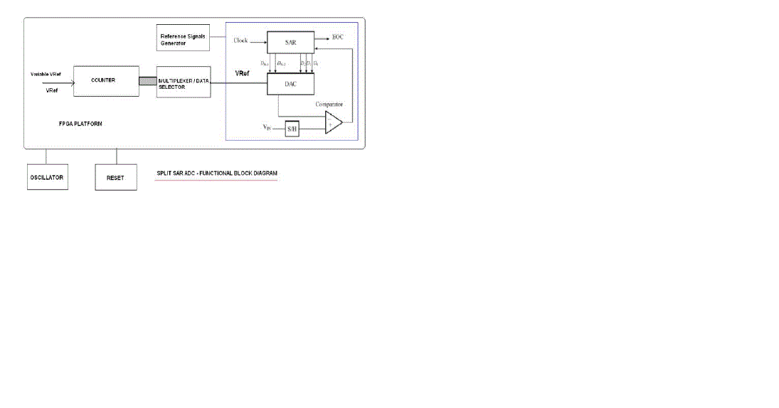
| In the proposed system we are planning to implement SAR ADC in a configurable manner with different
frequency inputs, the configurable means that the entire ADC architecture can work with different perfromance by
changing the Vref of the ADC. Normally in all ADC Vref , Vin , Vth plays. A major role in adc conversion, by varying
the values of Vref. we can change the performance of the ADC, We store the different values of Vref through
Multiplexer , for selecting the mux inputs we have counter, Reference signal generator generates different analog
signals to to test our ADC .SAR ADCs provide a high degree of configurability on both circuit level and architectural
level. At architectural level the loop order and oversampling ratio can be changed, the number of included blocks, and
way these blocks are arranged. At circuit level many things could change, such as bias currents, amplifier performance,
quantized resolution etc. |
3.1 BLOCK DIAGRAM |
| If an ADC is reconfigured in the way the blocks in the ADC are used and ordered, it is an architectural change of the
ADC, or architectural re configurability. These blocks can also be changed, for instance how the amplifiers are biased,
or how many bits of resolution that a quantise has in a SAR ADC.These are examples of how circuit level
reconfigurability is applied to an ADC. |
3.1.1 Module Description |
| In this first module we design the selective network for giving the appropriate input to the successive approximation
registers ADC and analyse the performance of the designed network. In this second module we design the sample
and hold circuit for processing the given analog signal from the selective network. Here after we measure the
performance of the designed circuit.In this third module we design the successive approximation registers logic for
effective analog to digital. |
3.2.3 SONDAE_APPLICATION |
| A Radiosonde (Sonde is French and German for probe) is a piece of equipment used on weather balloons that measures
various atmospheric parameters and transmits them to a fixed receiver. Radiosonde may operate at a radio frequency of
403 |
| MHz or 1680 MHz and both types may be adjusted slightly higher or lower as required. A raw in sonde is a
Radiosonde that is designed to only measure wind speed and direction. Colloquially, raw in sondes are usually referred
to as Radiosonde. Modern Radiosonde measure or calculate the following variables: |
| There are two primary purposes of upper-air soundings: to analyse and describe current weather patterns and to provide
inputs to short- and medium range computer-based weather forecast models. One very important, specialized use of
atmospheric soundings is in support of forecasting hurricane movement. Special Radiosonde called drop wind sondes
are launched from weather reconnaissance aircraft to observe atmospheric structure in the core of the hurricane as well
as in the area downwind of the storm itself. |
3.2.4 WIND FINDING |
| There are several techniques for measuring winds with only a balloon or with a combination balloon and Radiosonde.
When a Radiosonde measures winds it is called a radio-wind-sonde or rawinsonde. Radiosonde wind finding methods
vary widely. In all cases, the winds are determined byobserving the drift of the balloon. One class of wind measurement
techniques tracks the balloon externally using one of three methods: (1) optical systems use a the odolite to visually
track the balloon’s azimuth and elevation; (2) radio the odolites track a radio signal sent from a transmitter on the
Radiosonde, again to obtain azimuth and elevation information; and (3) radar systems track a radar retro reflector
suspended from the balloon to obtain slant range, azimuth, and elevation. |
III. EXPERIMENTAL RESULTS AND COMPARISON |
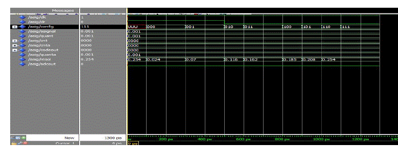
(i) Simulation Results of Analog Signal |
| Optical systems use a the odolite to visually track the balloon’s azimuth and elevation. |
 |
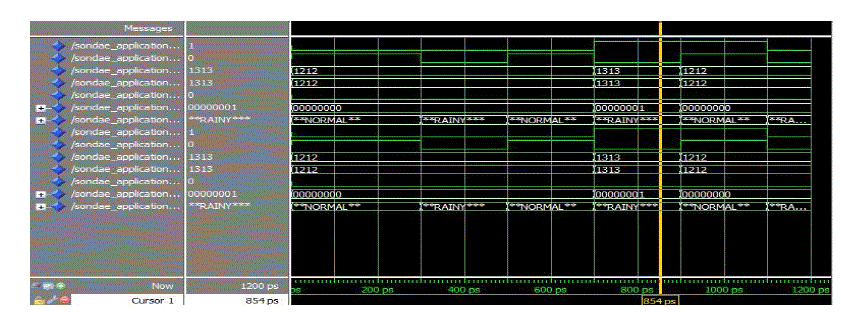
(ii) Simulation Results of Sondae Application |
| Radio the odolites track a radio signal sent from a transmitter on the Radiosonde, again to
obtain azimuth and elevation information |
 |
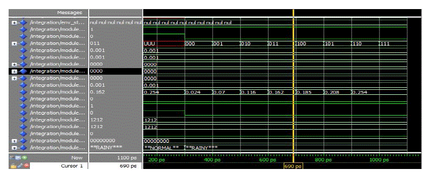
(iii) Simulation Results of Integration |
| Radar systems track a radar retro reflector suspended from the balloon to obtain slant range, azimuth, and
elevation. |
 |
IV. CONCLUSION |
| The SAR ADCs operating at tens of MS/s with conventional and VCM-based switching were presented. The linearity
behaviours of the DACs switching and structure were analysed and verified by both simulated and measured results.
The VCM-based switching technique provides superior conversion linearity when compared with the conventional
method because of its array’s capacitors correlation during each bit cycling. The reduction of the maximum ratio and
sum of the total capacitance can lead to area savings and power efficiency.Which allow the SAR converter to work at
high-speed while meeting a low power consumption requirement. The ADC achieves 1.46mW power consumption and
occupies only 0.012mm2.The measured performance corresponds to an FOM of 39fJ/conversion-step, which is
comparable with the best published ADCs. |
| |
Tables at a glance |
 |
 |
| Table 1 |
Table 2 |
|
| |
Figures at a glance |
 |
 |
 |
| Figure 1 |
Figure 2 |
Figure 3 |
|
 |
 |
 |
| Figure 4 |
Figure 6 |
Figure 8 |
|
| |
References |
- Split-SAR ADCs: Improved Linearity With Power and Speed Optimization, Yan Zhu, Chi Hang Chan, U-Fat Chio, Sai-Weng Sin, Seng-Pan U,Rui Paulo Martins, and Franco Maloberti, IEEE transactions on very large scale integration (VLSI) systems, Vol. 22, no. 2, February 2014.
- Y. Zhu, U.-F. Chio, H.-G.Wei,S.-W. Sin, U. Seng-Pan, and R. P. Martins, âÃâ¬ÃÅA power-efficient capacitor structure for high- speed charge recyclingSAR ADCs,âÃâ¬Ã in Proc. IEEE Int. Conf. Electron. CircuitsSyst., Aug.âÃâ¬ÃâSep. 2008, pp. 642âÃâ¬Ãâ645.
- Radiosonde Temperature, pressure, air for an Environmental StatusâÃâ¬ÃÂ, WF Dabberdt and R Shell horn, Vaisala Inc., Boulder, CO, USA, Copyright2003 Elsevier Science Ltd. All Rights Reserved, rwas.2003.0344 23/9/02 17:18 M. SHANKAR No. of pages: 14
- M. Saberi, R. Lotfi, K. Mafinezhad, and W. A. Serdijn, âÃâ¬ÃÅAnalysis of power consumption and linearity in capacitive Digital-to-Analog Convertersused in Successive Approximation ADCs,âÃâ¬Ã IEEE Trans. CircuitSyst. I, Regular Papers, vol. 58, no. 8, pp. 1736âÃâ¬Ãâ1748, Aug. 2011
- Y. F. Chen, X. Zhu, H. Tamura, M. Kibune, Y. Tomita, T. Hamada, M. Yoshioka, K. Ishikawa, T. Takayama, J. Ogawa, S. Tsukamoto, and T.Kuroda, âÃâ¬ÃÅSplit capacitor DAC mismatch calibration in successive approximation ADC,âÃâ¬Ã in Proc. IEEE Custom Integr. Circuits Conf,Sep. 2009, pp.279âÃâ¬Ãâ482.
- S.Wong, Y. Zhu, C.-H. Chinju.-F. Chio S.-W. Sin, U. Seng-Pan, and R. P. Martins, âÃâ¬ÃÅParasiticcalibration by two-step ratio approaching technique for split capacitor array SAR ADCs,âÃâ¬Ã in Proc. IEEE SOCDesign Conf. Int., Nov. 2009, pp. 333-336.
|