Phase locked loop is a familiar circuit for high frequency application and very short interlocking time. In this paper we have implemented and analysed All Digital Phase locked loop (ADPLL), as the present applications requires a low cost, low power and high speed Phase locked loops. The design is synthesized in Xilinx ISE software. The pure digital phase locked loop is attractive because it is less sensitive to noise and operating conditions than its analog counterpart. This project gives details of the basic blocks of an ADPLL. In this project it is been planned to implementation of ADPLL. Its simulation results are verified for all the corners of inputs. The ADPLL is planned for 200 MHz central frequency
Keywords |
| PLL, VCO,PFD, ADPLL |
INTRODUCTION |
| A modern advance technology in integrated circuit technology makes fabrication processes very suitable for
digital designs. Small-area and low-voltage designs are mandated by market requirements. Another advantage of
digital PLL is easy to redesign with the process changes. Since analog blocks are present in a number of digital and
mixed-signal ICs, their redesign is an important factor in the release of a new product. However, the performance
requirements of analog blocks necessitates a complete redesign in a new process, thereby increasing the design cycle
time. Reducing the amount of analog circuitry can improve the redesign of these mixed-signal ICs. A Phase Locked
Loop is mainly used for the purpose of synchronization of the frequency and phase of a locally generated signal with
that of an incoming signal. There are three components in a PLL. The Phase Frequency detector (PFD), the loop filter
and the Voltage Controlled Oscillator (VCO). The VCO is the heart of any PLL. The mechanism by which this VCO
operates decides the type of the PLL circuit being used. There are basically four types of constructing PLLs namely
Linear PLL (LPLL), Digital PLL (DPLL) and All Digital PLL (ADPLL). |
| The analog PLLs (APLLs) are still widely used, but digital PLLs (DPLLs) are attracting more attention for the
significant advantages of digital systems over their analog counterparts. These advantages include superiority in
performance, speed, reliability, and reduction in size and cost. DPLLs alleviated many problems associated with
APLLs. The following is a brief comparison: |
| 1. APLLs suffer from the sensitivity of the voltage-controlled oscillator (which decides the center frequency) to
temperature and power supply variations, hence the need for initial calibration and periodic adjustments. DPLLs do not
suffer from such a problem. |
| 2. the most familiar error detectors used in APLLs utilize analog multipliers (balanced modulators) which are sensitive
to d.c. drifts, a problem that does not exist in DPLLs. |
| 3. DPLLs can operate at very low frequencies that create problems in APLLs. These problems are related to the
operation of the analog low-pass filter in extracting the lower frequency component, as it needs larger time for better
frequency resolution, and this will reduce the locking speed. |
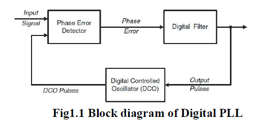
| 4. Self-acquisition of APLLs is often slow and unreliable; while DPLLs, a basic block diagram is shown in Figure 1.1,
have faster locking speeds. This is due to the basic operation of the analog low-pass filter and the analog multiplier in
the phase detector (PD). |
 |
LITERATURE SURVEY |
| A survey of PLL is presented by Gupta in his paper. Both classical and modem approaches are discussed. He
suggested that although the design of the A PLL is fairly well documented, more needs to be done to pinpoint the
formal design of the DPLL, the primary use of the PLL has been in more sophisticated communication systems,
however, with the rapid development of IC Technology, time is not far when PLL’s will be used widely in consumer
electronics.[Gupta somvanshi 1975]. |
| One of the important applications of Phase –lock loop is described by Yinqing. According to him Phase-lock
loops are widely used in carrier synchronization and bit synchronization systems to improve their synchronization
properties. Phase-lock loops are used in synchronization systems due to their tracking, narrow band filtering and
memory properties. [Yinqing,et.al, 1991]. |
| Another important application of Phase –lock loop as frequency synthesizer and its model is described by
Yang in 1997. Yang developed a model of a phase-locked loop (PLL) - based frequency synthesizer. The voltagecontrolled
oscillator (VCO) utilizing a ring of single-ended current-steering amplifiers (CSA) provides low noise, wide
operating frequencies, and operation over a wide range of power supply voltage. A programmable charge pump circuit
automatically configures the loop gain and optimizes it over the whole frequency range. The measured PLL frequency
ranges are 0.3–165 MHz and 0.3–100 MHz at 5 V and 3 V supplies, respectively. The peak-to-peak jitter is 81 ps (13
ps rms) at 100 MHz. The chip is fabricated with a standard 0.8-m n-well CMOS process. The chip is implemented in a
standard 0.8- m CMOS process. [Yang et.al, 1997] |
| From the continuous survey it is observed that foundry of technology and supply voltage range is continuously
decreases with the advancement of technology. Phase-lock loop with 0.35- m CMOS technology at a supply voltage of
1.8 V has been designed in 2002.Chen and Sheen presented a phase-locked loop for clock generation that consists of a
phase/frequency detector, charge pump, loop filter, range-programmable voltage-controlled ring oscillator, and
programmable divider. Circuits as having low power dissipation, is widely adopted. The modified phase detector and
charge pump have been extensively used to enhance the performance of the PLL. By applying the TSMC 0.35- m
CMOS technology, the proposed phase-locked loop that uses the power-switch scheme can yield clock signals ranging
from 103 MHz to 1.02 GHz at a supply voltage of 1.8 V. Moreover, power dissipation that is proportional to the
number of paralleled inverter rings is measured with 1.32 to 4.59 mW. By using the TSMC 0.35- m CMOS technology,
the designed PLL using the power-switch scheme can generate clock frequencies ranging from 103 MHz to 1.02 GHz
with a power dissipation ranging from 1.32 to 4.59 mW, at a supply voltage of 1.8 V. [Chen and Sheen, 2002] |
CLASSIFICATION OF DPLLs |
| Digital phase-locked loops can be classified into two major categories depending on the type of sampling
process. 1. Uniform sampling DPLLs 2. Non-uniform sampling DPLLs. The DPLLs can be also classified according to the mechanization of the phase
detector into five types as follows namely The flip-flop DPLL, The Nyquist-rate DPLL, The lead-lag DPLL (LLDPLL),
a.k.a binary-quantized DPLL and 4. Exclusive-OR DPLL Types 2 above belongs to uniform sampling, while
the others belong to non uniform sampling. A brief discussion of each type is given below. |
Flip-Flop DPLL |
| In this type the phase detector is realized by a set-clear flip-flop and a counter. The sinusoidal input signal is
converted into a square wave through an operational amplifier acting as a comparator. The output “Q” of the flip-flop is
set to logic “1” on the positive-going edge of the comparator, and to logic “0” on the positive-going edge of the digital
controlled oscillator (DCO). Hence the duration when Q is at level “1” will be proportional to phase error between the
input signal and the DCO. This error is used to gate the counter clock which has a frequency of 2Mfo where fo is the
center frequency of the DPLL and 2M is the number of quantization levels of the phase error over period of 2π. The
counter is zeroed and starts counting on the positive-going edge of the flip-flop waveform. The content of the counter,
No, which is proportional to the phase error, is applied to the N-bit first-order digital filter which consists of
proportional and accumulation paths. The output of the digital filter K controls the period of the DCO which consists
basically of a programmable divide-by-K counter. It is the phase of the input signal that undergoes non-uniform
sampling here rather than the amplitude. |
Lead-Lag DPLL |
| This type of DPLLs has been developed by the work in and extended in to include a second-order sequential
filter with memory. The LL-DPLL is characterized by the binary output of the phase detector that indicates whether the
DCO waveform leads or lags the input signal. Due to this quantization it is often named “binary quantized DPLL”. The
input sinusoidal signal should be converted to a square wave by a comparator. On the occurrence of a DCO pulse,
either “lead” or “lag” terminal of the phase detector will give a pulse depending on the state of the input signal being
“high” or “low”, respectively. These pulses are applied to a special type of digital filters known as “sequential filter.”
The sequential filter deals with the input “lead” and “lag” pulses statistically; it observes them for a variable duration of
time and gives a decision when a reliable limit is reached. |
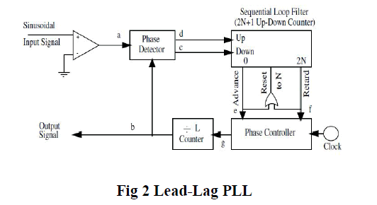 |
| Figure 2 shows that the sequential filter is composed of an up-down counter whose length is 2N + 1. A pulse at the
“lead” terminal causes the content of the counter to increase by 1, while the “lag” pulse behaves conversely. When the
content of the counter reaches 2N or zero, the corresponding “Retard” output gives a pulse that resets the counter to “N”
and triggers the phase controller. A “Retard” pulse causes the phase controller to delete one pulse from the clock pulse
train that is applied to the divide-by-L counter, forcing the DCO phase to retard by 2π/L, where L is the number of
quantization levels of the period 2π. An “Advance pulse does the contrary. When “lead” and “lag” pulses are equally
probable, a case that indicates locking, the counter cycle has maximum duration. Other types of sequential filters exist
like the N-before-M filter and the variable reset random walk filter. |
ARCHITECTURE OF ADPLL |
Phase Frequency Detector (PFD) |
| Phase detector generates error signals depending upon the phase error in locked state and frequency error in
unlocked state. We have used a synchronous version of PFD presented in [1]. This synchronous PFD can be easily
implemented on an FPGA as all signals are synchronized to a clock. |
Loop Filter |
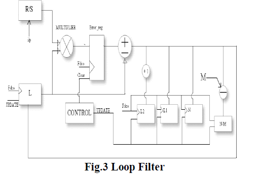
| Loop filter takes error signals from PFD as input, these signals are processed to generate control signals for
dco. Loop filter effectively performs the following calculations once on each cycle of dco clock period for duration of
mismatch. The implemented loop filter is presented in figure 3.This implementation is designed for low hardware
requirements and high frequency of operation. Fixed point arithmetic is used to accommodate fractional values. The
register error denoted in figure as ‘Error reg’ is included to enhance maximum frequency of operation. Including this
register requires change in generated control signals denoted in figure as ‘ clear’ and ‘up date’ so that equation 1 is
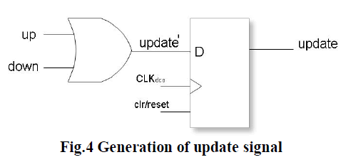
calculated for equal number of clk dco cycles for which phase error exist. The required change is that update and clear
signals must be delayed by one clk dco cycle which has been represented in figure 4. |
 |
 |
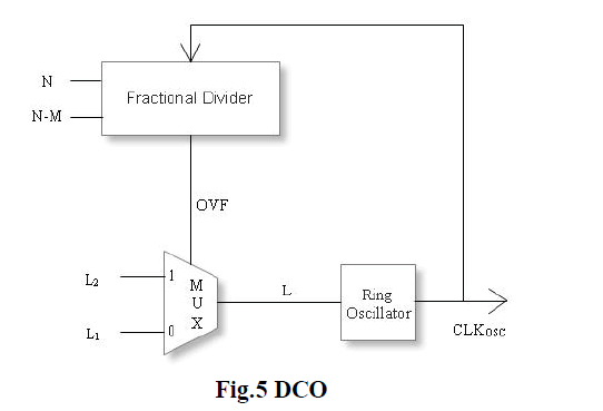
DCO |
| We have implemented dco proposed in which comprises of two parts. A ring oscillator with variable delay, the
second part consists of control unit that constantly switches number of delay elements in the ring between two adjacent
integral values to obtain fractional number of effective delay elements. This implementation has high frequency
resolution. Switching between two adjacent values causes maximum peak to peak jitter of. Complete architecture of
DCO is shown in figure 5 |
 |
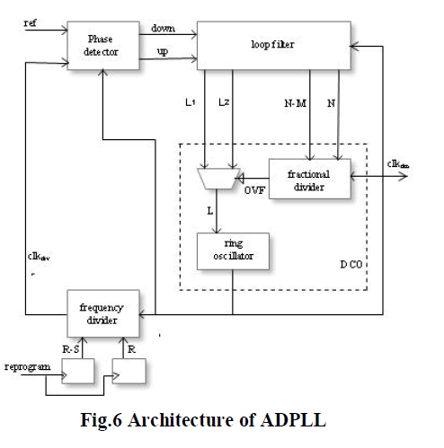
Fractional Frequency Divider (FFD) |
| For high frequency resolution and flexibility the feedback of DCO has been implemented using a
reprogrammable fractional frequency divider presented in [2]. Scaling factor of this accumulator switches periodically
between two adjacent integers realizing a fractional scaling factor on average. The Most Significant Bit (MSB) of
register is the output of FFD. The MSB also controls selection of N or N-M values. If MSB is zero, negative value N-M
is selected. If MSB is one, the positive value N is selected. On average MSB bit is high for N out of M cycles of
clkdco. The register N and N-M are made reprogrammable using a separate clock signal ‘reprogram’. The values of
these registers can be varied so as to attain different clkdco frequencies for different ref frequencies as per requirement.
A complete architecture is shown in below Fig.6 |
 |
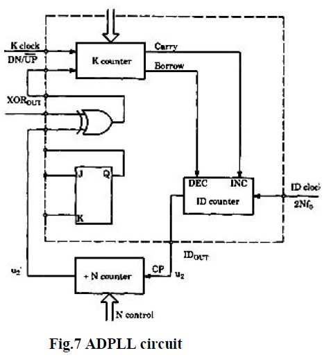
IMPLEMENTATION USING VERILOG |
| ADPLL components are Phase Detectors (PDs), Loop Filters (LFs) and Digital Controlled Oscillators (DCOs).
Based on all these components we can design various types of ADPLLs. For designing ADPLL, Verilog hardware
description language is used. It is simulated in ISE Xilinx 12.1. All basic building blocks of ADPLL i.e. Phase Detector
(PD), Loop Filter (LF) and Digital Controlled Oscillator (DCO) are designed using Verilog (HDL). EXOR gate and JK
Flip flop are used as PD. Output of EXOR or JK Flip-flop PD is fed into K counter. This signal is represented by
Dn/up. K counter clock is Kclk signal. Kclk is M time multiple of center frequency. Up counter and down counter are
two independent counters of K counter. The Dn/up signal controls the K counter. If this signal is low then up counter is
active and down counter becomes inactive. In other case when this signal is high then down counter is active and up
counter becomes inactive. Outputs of K counter are carry and borrow pulses. Carry and borrow are MSB of the up and
down counter respectively. Carry pulse is fed into INC input of ID counter .Whereas borrow pulse is fed into DEC
input of ID counter .Output of ID counter is IDout .In general one carry pulse adds half cycle to IDout and one borrow
pulse delete half cycle to IDout signal.ID clock is 2N time multiples of center frequency. Output of ID counter (IDout)
is fed into divide by N counter, which is the last stage of DCO.ID out is used as clock pulses for divide by N counter.
Design is verified and simulated in Xilinx ISE 12.1 tool. A diagram of designed and implemented ADPLL [8] is shown
in the Fig.7. Also M=2N, so both clock frequency are taken from the same source. |
 |
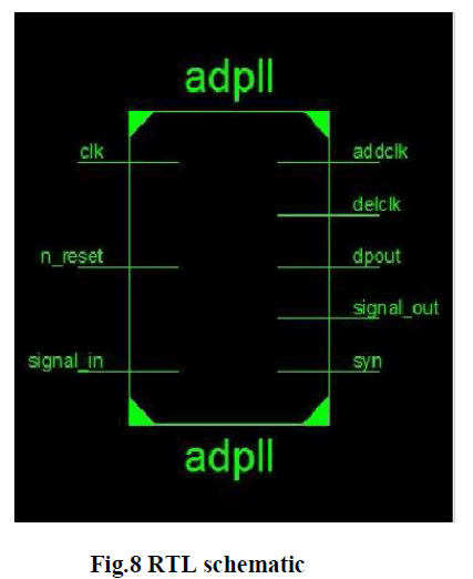 |
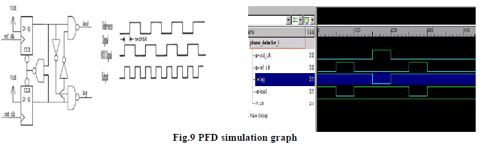
SIMULATION RESULTS |
| Phase frequency detector and DCO simulations are done using Xilinx and simulation waveform of same is shown
below. The design has been done keeping in mind the portability, flexibility and optimality criterion. It can be used in
any design suiting the given frequency specifications. A system clock of 5 MHz is used. The design is implemented for
a center frequency of 300 kHz. It’s mainly meant for low frequency applications. The current design offers a operating
frequency range of 290 kHz to 320 kHz approximately. The top module of the designed ADPLL has been presented in
Fig 8. The design can be extended beyond that also. But the logic criterion needs to be changed to overcome the
propagation delay that is introduced due to greater number of bits involved in the computation. |
 |
CONCLUSION |
| According to review of ADPLL, digital circuits are more versatile, efficient, flexible, and less noisy as
compared to analog circuit. This paper discusses the ADPLL design using Verilog HDL It also presents the FPGA
implementation in detail. The ADPLL blocks used for the design are also given here. This PLL is designed for the centre
frequency of 200 kHz and its operating frequency range of ADPLL is 189 kHz to 215 kHz, which is the lock range of the
design. When the input was at fault, it automatically resumed output formation by employing the last known correct
parameters. |
References |
- Aniruddha Chandra, Lecture on “Phase Locked Loop”, in winter school on VLSI Systems Design , ECE Department, NIT Durgapur, Jan. 2009
- KusumLata Department of Electronics and Communication Engineering, Indian Institute of Information Technology,Allahabad, INDIA
- Manoj Kumar Department of Electronics and Communication Engineering, Indian Institute of Information Technology, Allahabad, INDIA
- Phase-Locked Loops: Design, Simulation & Applications By Roland E. Best, 4th Edition, McGraw-Hill Professional Engineering.
- Martin Kumm, HaraldKlingbeil, Peter Zipf, “An FPGA Based Linear All-Digital Phase-Locked Loop”, IEEE Trans. on Circuits and Systems57-I(9): 2487-2497 (2010).
- Kwang-Jin Lee, Hyo-Chang Kim, Uk-Rae Cho, Hyun- GeunByun, Guki Kim, “A Low Jitter ADPLL for Mobile Applications”, IEICE Transactions 88-C(6), 1241-1247 (2005).
- Ping-Hsuan Hsieh, Jay Maxey and Chih-Kong Ken Yang, “A Phase-Selecting Digital Phase-Locked Loop With Bandwidth Tracking in 65 nm CMOS Technology,” IEEE Journal of Solid-State Circuits, vol. 45, no.4, pp.781-792, April 2010.
- Chia-Tsun Wu, Wen-Chung Shen, Wei Wang and An-Yen Wu, “A Two-Cycle Lock-In Time ADPLL Design Based on a Frequency Estimation Algorithm,” IEEE Transaction on Circuits and Systems-II, vol.57, no.6, pp.430-434, June 2010.
- LianggeXu, SaskaLindfors, Kari Stadius and JussiRyynanen, “A 2.4-GHz Low-Power All-Digital Phase-Locked Loop,” IEEE Journal of Solid-State Circuits, vol.45, no.8, pp.1513-1521, Aug 2010.
- B. Razavi, “Monolithic phase-locked loops and clock recovery circuits- theory and design”, IEEE Press,pp. 283-377 and 381-483, 1996.
- B. P. Panda, p. K. Rout, d. P. Acharya and g. Panda “Design of a novel current starved VCO via constrained geometric programming” april 12-14 2011 international symposium on devices mems intelligent systems communications 2011
|