Keywords
|
| Scan FF(S-FF), Built-in self-test (BIST), linear feedback shift register (LFSR), Single cycle access (SCA). |
INTRODUCTION
|
| The standard shift scan (SS) method is the most popular test implementation within the last decades. It has been tried to improve this approach in terms of test time, test data volume and test power by optimizing the scan pattern, using different scan chain structures, different scan support logic, or a combination of these modifications. |
| A. Conventional Scan Design. |
| Scan is a design technique that converts sequential logic to combinational logic. Scan design effectively converts a sequential logic (clocked) design to a combinational logic (non-clocked) design allowing ATPG tools [2] to produce high fault coverage test vectors efficiently. It enables a complex circuit to be partitioned into individual combinational logic functions, each logic function can be tested separately, and all sequential logic elements can be directly controlled. Sequential logic circuits can require extensive conditioning which is both time consuming and expensive in terms of simulation and test time. To implement a Full Scan Design, each flip-flop within the design is converted to a specialized Scan flop. Scan flops are easily controlled, and become additional inputs and outputs, similar to adding internal test points. A circuit is considered to be a Partial Scan Design when Scan Flip-Flops are used, but not to the extent that allows full control of the entire circuit. Scan connects all state elements (flip-flops) of a design into one, or multiple shift registers which are referred to as Scan Chains. Scan flops may also be added to any internal circuit paths that contain feedback signals in order to allow direct control of the fed back signal path. Feedback paths are sometimes referred to as Secondary State Variables. |
| Once the Scan chain is configured, it allows both controllability and observability over the entire circuit, assuming a Full Scan design. For ATPG purposes [6], the Scan flip-flops are considered virtual inputs and outputs. During Scan test, input data is shifted serially into the device and then applied in parallel to all inputs of the target logic blocks. Outputs of the logic blocks that are not directly accessible, via primary outputs, are captured in parallel into the Scan chains, then shifted out serially for evaluation. This method of testing greatly reduces the number of data cycles required to condition and test the logic when compared with using only the primary inputs and outputs. It also improves the diagnostic capabilities of the test. |
| B. Non Scan Logic |
| Figure.1 illustrates a simple circuit containing several blocks of logic, each with its own function, and the associated sequential logic shown as “FF” (flip-flops) [5]. Ideally each logic block will be exhaustively tested for faults. From the diagram you can see that the inputs to Block A can be directly controlled via the primary inputs, but the output response must propagate through Blocks B, and C before being observed on the primary outputs. Logic Block B can be neither accessed nor observed directly. Block C’s outputs can be observed, but the inputs cannot be directly accessed. This design makes it difficult to achieve high fault coverage with a limited number of clock cycles. |
| If any block within the circuit fails, the ability to diagnose or localize the problem is very limited. This circuit would be much easier to test, and troubleshoot, if each logic block could be independently controlled and observed. Inserting Scan logic into this circuit will overcome these problems. Inserting Scan logic involves several modifications to the circuit. First, let’s look at how the flip-flop design is modified to become Scan enabled. |
| C. Scan Logic |
| Figure.2 shows the same circuit as Figure. 1 on page 2 only with Scan logic inserted. Notice that each D flop has been modified to a Scan flop, then linked together to form a chain. Three pins have been added: Serial Data In (SDI) connected to the mux input of the first flop in the chain, Serial Data Out (SDO) connected to the output of the last flop in the chain, and Scan Enable (SE) connected to the mux control of each flop. This circuit can now be tested using the Scan chain. Logic Block A can be tested by applying data to the primary inputs then capturing the results into the first 4 flops (closest to SDI), this is accomplished in normal functional mode (SE set low). Once the results are captured the SE pin will be set high (Scan mode), and the captured data shifted and observed at the SDO pin. To test Logic Block B, input conditioning data can be shifted into the first 4 flops (SE high). |
| SE is then set low, and the chip goes into normal operational mode, the data propagates through the combinational logic and is captured into the Scan flops located at the output of Block B on the next clock. Once the data is captured, SE is set high and the data is shifted (clocked) through the Scan chain and observed at SDO. During this test the first four flops act as conditioning inputs, the next three flops act as observation points (outputs). It is possible to test all logic blocks at the same time. This test begins by applying conditioning data to the primary inputs for Block A. SE is then set high and conditioning data is shifted into the entire Scan chain. SE is set low and the test results are captured and primary outputs evaluated. SE is set high and the results shifted out. The first four flops act as both inputs for conditioning Block B, and as outputs for observing the results of Block A. The remaining flops act as inputs to condition Block C. |
| Converting normal flops to Scan flops greatly increases the effective number of inputs and outputs. Replacing the normal flip-flops with Scan flops may have a negative impact on the operating speed of the circuit. Adding Scan logic also increases die size and pin count, it reduces yield and complicates the routing of interconnect wiring. Like many issues in test, it is a cost/benefit trade off. |
PAPER ORGANIZATION
|
| This paper is structured as follows. In Section III, “SCAh-Structure with Hold Mode” the single cycle access test structure is explained. The feasibility, area, test cycles, power consumption, and debugging capabilities of this solution is compared to alternative state-of-the-art methods. In Section IV, “SCA-Structure without Hold Mode” demonstrates further solutions to overcome the area disadvantage of the proposed method. The advantages of the SCAh-structure and the lower area overhead of the SCA-structure are combined and presented in Section V, “Gated SCA-Structure”. Sections VI, “Page-Setup For SCA-Structure ”. Sections VII, “Experimental Results ” and VIII, “Conclusion”. |
SCAH-STRUCTURE WITH HOLD MODE
|
| A. SCAh-FF |
| The key element of the single cycle access structure with hold mode (SCAhS) is the signal cycle access register (Flip-Flop, FF) with hold mode (SCAh-FF) [1]. It is based on a standard scan register (S-FF) and uses two more 2-to-1 multiplexers. The new SCAh-FF can be seen in Fig. 3. The SCAh-FF has one more input and one more output compared to the standard shift register (S-FF). The inputs clock {clk}, data-in {di}, and scan-in {si} still exists. The scan-enable is now a 2 bit bus {se[0:1]}. An additional scan output pin {so} is added. The reset input and inverse output pins are not shown. Based on [1]. The internal logic enables the register to run in one additional hold mode, whereas the additional output multiplexer can bypass the register to directly drive the value of {si}. The resulting functionality is best explained by a truth table (see Table 1). |
| In functional mode {se[0:1]==00} , the register captures {di} and {si } follows {so } (usually stable). In read mode { so } has the value of {do} so that {do} can be read out asynchronously. In the event of the relevant clock edge, the register captures {di }. |
| In hold mode, { so } follows {si }, and the register remains in the state {do}, capturing its own value. When{se[0:1]==11} , the registers captures { si} and {so } changes to the new value of {do } (sync. write/read mode). The slave latch of a FF is usually connected to the output driver of the data-out pin and/or an inverting driver for the inverse-data-out pin. The internal multiplexer for the SCAh-FF (shown in Fig. 3) can also be driven by this slave latch output. The fan-out number of the data-out pin (or inverse-data-out pin) refers to the number of input pins which are driven by the SCAh-FF data output drivers. |
SCAH-STRUCTURE WITHOUT HOLD MODE
|
| A. SCA-FF |
| In order to reduce the area overhead of a SCAhS, a simpler SCA-FF is discussed. It adds only one 2-to-1 MUX to the standard S-FF (see Fig. 3) [1]. It only has one input, which is connected to the individual line-select signal. The pin which is connected to the global enable signal in the SCAhS is removed, so that the complete global scan enable tree becomes obsolete. The SCA-structure (SCAS) connectivity and page organization equals the one of the SCAhS (see Figs. 4 and 7) without the global scan enable {gse }. |
GATED SCA-STRUCTURE
|
| This section discusses the gated SCAS (gSCAS) [1], which has all the benefits of the SCAhS but only has the area overhead of the SCAS. The hold function of the SCAh-FF is missing in the SCA-FF. It is instead built into the gated clock tree of the gSCAS. Fig. 6 shows the connectivity of the gSCA. The scan path reaches from the scan-in ANDselector over the SCA-FF chain (by connecting the scan-out pins of each SCA-FF with the scan-in pins of the succeeding SCA-FF) and is connected with the input of the XOR-tree. The individual line-select signals {ls } are connected with the { se} input of the SCA-FF in the relevant line. All SCA-FF on a line are clocked by a gated clock element (gcl). The gcl is driven by the clock and the line-select signal. The gated clock element can be enhanced, if a clock enable signal ce generated by combinatorial logic exists. The global scan enable signal is connected with each gcl, which is already the case in SS if gated clock elements are used to propagate the clock during shift. |
PAGESETUP FOR SCA-STRUCTURE
|
| The SCAS enables single cycle read/write accesses to the individual register line [1]. The test structure is now organized in pages to achieve a read/write access at design speed or at a reasonable test speed. The page depth equals the scan chain depth (SD = number of SCA-FF connected to one chain on one page). Assuming it is 31. Multiplied with the scan width (SW = number of scan chains on one page, for instance 32), the resulting number of SCAh-FF is (SD*SW=) 992 per page. |
| In this rather extreme compact case, the page uses a global 1-out-of-31 address line decoder. A page selector {psel } selects the individual page and drives the scan input bus signals and line select {ls } signals (AND-ed) only of this particular page. {psel } can be driven by a register which is set by a dedicated test control logic. If not selected, the page remains inactive to reduce activity. The scan output buses of all pages {so } are bit-wise XOR-ed with the {so } of other pages to generate the global scan-out bus pso . If the page is inactive, the XOR-tree passes the value of previous pages unchanged since all {so} bits of an unselected page are “0”. |
| With the page organization, the relevant timing paths become clear. During a read, the registers are selected by the line-select signal and drive the scan-out bus {so} through a multiplexer chain of the succeeding registers and the pagescan- out bus {pso } through the XOR-tree. During a write, the scan-in bus {si } values are passed through the ANDselector and the multiplexer chain of the trailing register to the registers of the selected line. In order to achieve a high test speed, the test implementation can be pipelined. The scan-in bus {si } and the line-select {ls } outputs of the global address-decoder can be registered. Also the XOR-tree can be pipelined with buried register sets. For eight pages a logic depth of three XOR-cells can be reached. |
| If an optimal test speed cannot be achieved, the scan-depth SD can be reduced (to any number). It is important to notice, that there is no timing path between adjacent registers on the scan chain during test mode ({so }ïÃÆà{ si}). Therefore, no hold time problems exists, which are known from shift-scan-test, and no buffers must be inserted for hold time fixes. |
| To analytically evaluate the power consumption of the gated clock approach applied to a LFSR [3], we have to take into account also the dissipation introduced by the extra gates that are employed to implement the gated clock circuits, as well as the load effects introduced by these gates with respect to the traditional one. |
| In order to evaluate the power reduction obtained by applying the gated-clock approach to a SCA without hold FF, we have to analytically compare relationships (2) with (6). As a preliminary results, we obtained that. |
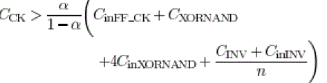 |
| which defines the technological condition (and the circuital solutions for the gate’s implementation) so that the gateclock approach leads to an improvement in terms of power reduction compared to the traditional S-FF and both SCAFF implementation. |
PERFORMANCE ANALYSIS
|
| Area will be increased considerably in case of Global SCA as compared to SCA without hold page due to AND gates usage in the design. But overall power dissipation will be reduced due to gated clock used in the whole page set up. |
| Single cycle access feature is shown in fig[8] by stimulated result. This is main difference between conventional shift scan design and our SCA design. This eliminates unwanted switching activity, so power dissipation is reduced. |
CONCLUSION
|
| A single cycle access structure is discussed. Various implementations with and without hold mode as well as gated and partial implementation methods are presented. We proved the power and area optimization using QUARTUS II EDA tool. Initially we implemet these scan FF in benchmark circuits and we implement BIST in vedic multiplication and finally we proved single cycle access features using model simulation results. |
ACKNOWLEDGMENT
|
| We take this opportunity to express our deepest gratitude and appreciation to all those who have helped us directly or indirectly towards the successful completion of this paper. |
Tables at a glance
|
|
|
Figures at a glance
|
 |
 |
 |
 |
| Figure 1 |
Figure 2 |
Figure 3 |
Figure 4 |
 |
 |
 |
| Figure 5 |
Figure 6 |
Figure 7 |
|
References
|
- Tobias Strauch , "Single Cycle Access Structure For Logic Test", IEEE Transactions On Very Large Scale Integration System, May 2012.
- H. Ando, “Testing VLSI with random access scan,” in Proc. Diag. Papers Compcon 80, 1980, pp 50-52.
- S. Almukhaizim and O. Sinanoglu, “Dynamic scan chain partitioning for reducing peak shift power during test,” IEEE Trans. Comput Aided Des.Integr. Circuits Syst., vol. 28, no. 2, pp. 298–302, Feb. 2009.
- N. Ahmed, M. Tehranipoor, C. Ravikumar, and K. Butler, “Local at-speed scan enable generation for transition fault testing using low- Cost tester”, Feb. 2009.
- J. Rajski, J. Tyszer, M. Kassab, and N. Mukherjee, “Embedded deterministic test,” IEEE Trans. Comput.-Aided Des.Integr. System”, pp. 776–792, May 2004.
- D. Czysz, M. Kassab, X. Lin, G. Mrugalski, J. Rajski, and J. Tyszer, “Low power scan shift and capture in the EDT environment,”
|