Keywords
|
| III-V Semiconductors, Solar cells, Optoelectronic. |
INTRODUCTION
|
| Solar energy is extensively studied as an endless, reliable and safe energy source. It is particularly important to increase the photovoltaic (PV) conversion efficiency from the viewpoints of both basic science and practical applications. [1]. The InGaN alloy system offers a unique opportunity to develop high efficiency multi-junction solar cells. A single junction solar cells made of Inx Ga1–xN have beens uccessfully developed, with x = 0, 0.2, and 0.3. The materials are grown on sapphire substrates by molecular beam epitaxy (MBE). The structure consists of a Si-doped InGaN layer, an intrinsic layer and an Mg-doped InGaN layer on the top [2]. InxGa1-xN alloys possess a bandgap ranging from the near infrared (0.7eV) to the ultra violet (3.4eV) [3]. This range corresponds very closely to the solar spectrum one making InxGa1-xN alloys promising candidates for radiation-resistant multi-junction solar cells [4]. |
| Materials with a bandgap energy Eg< 1.4 eV grown on GaAs substrates are of major interest for optoelectronic devices like multi-junction solar cells [5], 1.3 μm wavelength emitting lasers [6]. The ternary Ga1-xInxAs is an attractive material with a bandgap ranging from 1.44 eV for GaAs decreasing to 0.35 eV for InAs. Unfortunately, the lattice constant of this material also changes significantly when we modify the composition. Besides, lattice-matched substrates are not available for most Ga1-xInxAs compounds. This letter is the first report on the successful deposition of Ga0.35In0.65 P/Ga0.83In0.17P tandem solar cells grown lattice mismatched to the GaAs substrate material. Even though the amount of dislocations was determined to be in the order of 107cm-2; an excellent electrical performance of the device was achieved. The quantum efficiency was comparable to the lattice matched Ga0.51In0.49 P/GaAs tandem solar cells [7]. GaInP/GaAs tandem cells currently represent the highest efficiency monolithic solar cells and are in commercial production for space applications [8]. Strained semiconductors can be successfully incorporated into photovoltaic devices, as long as the critical thickness is respected for each separate layer as for the whole structure [9]. |
| Metal/semiconductors heterojunctions (SC) and SC A/SC B have a great impact on the realized PV solar cells. The electronic structure of the interface determines the electronic behavior of heterojunctions and Schottky barrier height [10]. In our work, we have used indium/gallium-based compounds to prepare our structures. With these materials we are able to prepare different alloys by adding III-V compounds. Ternary alloys like Ga(1-x)InxP and InxAs(1-x)P or quaternary compound like InxGa(1-x)AsyP(1-y). In this type of materials, the forbidden band width could be changed which means that optical properties could be altered and improved at a certain spectral wavelengths range. |
II.THEORY
|
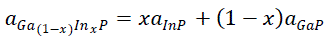
| III-V semiconductors like GaAs and InP tend to have a sphalerite (Zinc blende) structure when they crystallize. This type of structure is made exclusively of III-V atoms where we will have, stoichiometrically, one atom from column III elements corresponding to another atom from column V elements. As a result, strong covalent chemical bonds are obtained when one electron is shared between the atoms belonging to the group III elements and those of group IV. These bonds exhibit also weak ionic characteristics resulting from a difference in electronegativity between elements of group III and group IV. Let the lattice parameter „aâÃâ¬ÃŸ be the distance between two adjacent lattices. For alloys made of different semiconductor materials, the lattice parameter varies linearly with the different binary elements composition in accordance with Vegard law. For ternary elements Ga1-xInxP, the lattice parameter aInGaP is given by equation [11]. |
 |
| Semiconductors are characterized by an energy gap separating the conduction band from the valence band. This gap, called forbidden band, correspond to the energy needed for an electron to jump from the valence band to the conduction band. This energy could come from incident photons or electric excitations. This gap energy is equivalent to the energy provided by the system after the electron-hole recombination. The emission and detection phenomenon of photons is based on the detection of photons. When a material is grown on a substrate and if they possess different lattice parameters, there will be a parametric disagreement between the two lattices. This could be addressed depending on two cases: |
| 1. If the grown films are very thin, their lattice will be distorted elastically in a manner where the material lattice parameter will fit with the substrateâÃâ¬ÃŸs one in a direction parallel to the interface. In the direction perpendicular to the growth interface, the lattice will be distorted either by having either an elongation or a contraction depending if the thin film lattice parameter is smaller or bigger than the substrateâÃâ¬ÃŸs one respectively. In this case, the layer is being totally strained. |
| 2. For a thick epitaxial layer, the distortion of the materialâÃâ¬ÃŸs lattice is not sufficient to balance the mechanical energy and stress generated during the thin film growth. This disagreement is compensated by dislocation generated at the interface during the growth. These dislocations will spread from the substrate to the growth interface followed by a layer relaxation. |
| We have used Van and Walle model and Krijin formalism [12] to describe the effect of this strain-related phenomenon. The consequences of the constraints on the valence band and conduction band could be divided in two parts: |
| ïÃâ÷ Hydrostatic component: it is related to the strain along the growth axis. It induces a shift in the center of gravity for both the valence band and the conduction band. |
| ïÃâ÷ Shear component: it leads to the lifting and increase in the degenerate energy levels for light and heavy holes at K=0. |
III. SOLAR CELL STRUCTURE
|
| We have realized a solar cell using N-type Ga(1−x)InxP epitaxially grown on P-type GaAs. We have followed by the deposition of a thin Tin oxide (SnO2) film that replaces the metal layer and acts as window layer and antireflective coating due to its interesting optoelectronic characteristics (gap = 3.6 eV, refractive index 1.9-2.0). the last step is the deposition of silicon (Si) thin layer which have a large forbidden band of 9eV with a high resistivity of (1016Ω. cm) that gives her good insulating properties (Fig. 1). |
| Under light illumination, the generated electrons-holes pairs are directly separated by the internal electrical fields which yield a photocurrent density jph . Two types of electrical fields are produced; one at the depletion region of the MIS contact and the other field is located at the contact depletion region of semiconductor 1 and semiconductor 2. |
| Figure 2 shows the band diagram of SnO2/SiO2/GaInP/GaAs solar cell under illumination and at equilibrium. The insulating layer inserted between the metal and the semiconductor leads to the decrease of the thermoelectronic current as a result of the higher Schottky barrier. Concerning the Ga1−xInxP / GaAs interface, we have noticed that the two semiconductors have different conduction band energies and valence band energies. |
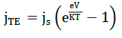
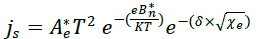
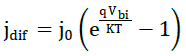
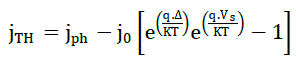
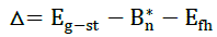
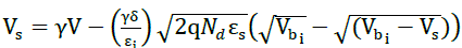
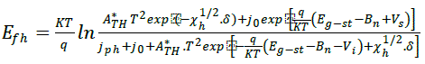
| The electric potential difference V of the illuminated solar device is the sum of two components: Vi, generated at the insulating layer and Vs, produced at the depletion region of the semiconductor. The difference of potential is then V=Vs+Vi. The voltage Vi heightens the barrier between SnO2 and GaInP which will make difficult for electrons to pass through by thermal effect B*=Bn+Vi . A higher barrier means that tunnel effect is the common mechanism for electron to get through the insulating layer. The current density in the SnO2/SiO2/GaInP structure is: J=JTH-JTE. Thermoelectronic current density is given by: |
 |
| and the saturation current : |
 |
| where , |
| δ: thickness of insulating layer |
| χe : electron in affinity. |
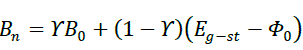 |
| ïÿýïÿý0:Level measured from the peak of the valence band to the highest occupied interface level. In general, this energy is equal to (Eg 3)[13]. |
| Eg-st: strain gap [14] |
| Y: denotes the influence of the interface states on the Schottky barrier. |
| B0: Schottky barrier. |
| Minority carrier diffusion current is given by: |
 |
| The diffusion voltage in the first loading area Vbi is given by =B0-Vn |
| where Vnrepresents the voltage difference between conduction band and Fermi level. |
| The current resulting from the passage of holes generated in the semiconductor and moving through the insulating layer to the metal by tunnel effect is given by the equation below: |
 |
 |
 |
| εi : Insulating layer dielectric constant. |
| Ds : Interface state density |
| q : Electron charge. |
| ïÿýïÿýïÿýïÿý : Bulkdonordensity. |
| εs : Dielectricconstant of the semiconductor. |
 |
| ïÿýïÿýïÿýïÿýïÿýïÿý ∗ : Holes Richardson constant (32A/cm2K2) |
| ïÿýïÿýïÿýïÿý : GaInP semiconductor holes affinity |
| DP: Holes diffusion constant. |
| LP: Holes diffusion length. |
| Vbi:Diffusion volt agein w1 |
IV. ELECTRICAL CHARACTERISTICS OF THE SnO2/SiO2/GaInP/GaAs SOLAR CELL
|
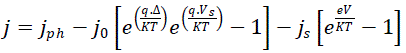
| In the electrical characterization of solar cells, we have to extract Current-Voltage J(V), curves under illumination condition and calculate the maximum power delivered by the device and its light conversion efficiency. The current density of the structure is given by the equation: |
 |
| The short-circuit current (ïÿýïÿýïÿýïÿýïÿýïÿý ) of the solar cell is expressed: |
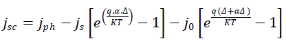 |
| α: absorption coefficient of the semiconductor. |
| Open-circuit voltage Voc of the solar cell is the sum of two voltages :Voc=Voc1+Voc2 . |
| Voc1of SnO2/SiO2/GaInPstructure is given by: |
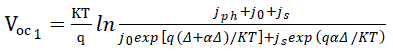 |
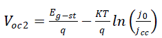
| Voc2 of the Ga(1−x)InxP/GaAs heterojunction structure is given by: |
 |
| The photocurrent density crossing the MIS device is expressed by the equation below [15]: |
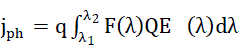 |
| F λ : is the solar spectrum AMG1.5, λ1and λ2 are wavelengths limits of absorbed solar spectrum. Taking into account the multiple reflections of light in the front and rear surfaces of the solar cell, optical electron-hole pairâÃâ¬ÃŸs generation rate is expressed in the following: |
 |
| Where R λ is the surface spectrumreflectivity, the first exponential factor results from the attenuation of light in the precedent layers of the cell, αi and zi are respectively the absorption coefficient and the width of the precedent layers. It is noted that in our case, the upper layers are SnO2 and SiO2 which possess an absorption coefficient (αi = 0),αGaAs and LGaAs are the absorption coefficient and the width of the bulk material GaAs, αGaInP and ïÿýïÿýïÿýïÿýïÿýïÿýïÿýïÿýïÿýïÿýïÿýïÿýïÿýïÿý are respectively the absorption coefficient and the width of the top lattice layer. |
V. RESULTS AND DISCUSSION
|
| Figure 3 shows the variation of the band energy gap vs Indium content. We have noticed that the gap decreases with increasing indium concentration whereas the strain (Ãâ°Ãâº) decreases. For In concentration x=0.48 (lattice matching), the gap equals 1.73eV but for x ïÃâ¬Ã¾ 0.48 the uniaxial compression gap is less than à 1.73eV with the strain Ãâ°ÃâºÃ¯Ãâ¬Ã¾0. In the opposite, for x< 0.48, extensive strain is superior to1.73 eV with Ãâ°Ãâº< 0. An example given is for x=0.90, the strain is Ãâ°Ãâº= 2.98% with the strain gap being Eghh-st=1.46eV. We have maximum structure absorption in the case of a compressive strain as found elsewhere [16]. |
| Figure 4 shows the variation the absorption with incident light energy hν. The absorption increases with higher Indium content. In the case we have a compressive constraint; the absorption is more significant than the case of a lattice match in gand extensive strain. For example, if Ãâ°Ãâº=3.3% the maximum absorption is αmax=2.35.105cm-1 but diminishes to αmax=7.76.104 cm-1 for Ãâ°Ãâº=-2.53%. That is a lattice matching-related increase of Δαmax=1.44.105 cm-1. |
| In figure 5, we show the J(V) characteristics for different In concentration. For higher In concentrations, we notice that current density (Jcc) decreases while the open circuit voltage (Voc) increase. The opposite happens in an extensive strain case (Ãâ°Ã⺠<0), Jcc is at a maximum and Voc is minimal. The opposite effect is obtained for a compressive strain (Ãâ°Ã⺠>0) and where we can see that he fill factor (FF) increases. |
| Figure 6 shows the variation of the structure power with the voltage. The maximum power delivered by the solar cell augments with higher compressive strain and lowers with an extensive one. For example, in the case of lattice matching (Ãâ°Ãâº=0), the maximal power amounts to 42.8mW but if we increase the strain to 3.3% the power reaches 48.83 mW that is an increase of ΔPmax=6.03mW. |
| Figure 7 depicts the efficiency (ïÃÂè) evolution of the GaInP/GaAs structure vs the strain Ãâ°Ãâº. It is clearly seen that ïÃÂè increases when the strain increases. The solar cell efficiency is maximum when Ãâ°Ãâº>0 and is higher for thicker SiO2 insulating layers. For a deformation of 3.3% and a thickness of δ= 50ÃËæ we will have an efficiency of 26.8%. For example, if we consider a GaInP/GaAs structure with a 50ÃËæthick insulating layer and a deformation Ãâ°Ãâº=1.21%, having an efficiency η=23.17%, raising the deformation to Ãâ°Ãâº=2.98% will raise η to 26.6% the is a relative amelioration of Δη = 3.43%. If we keep the deformation constant at Ãâ°Ãâº=1.21% and let the SiO2 insulating layer thickness vary between 10 and 50ÃËæ, the efficiency get boosted by Δη=6.97%. |
| Figure 8 represents the variation of the quantum efficiency (EQE) vs wavelength where we can see that EQE of the GaInP structure reaches 92%. The width of the absorption becomes larger when the strain varies. For an extensive strain of Ãâ°Ãâº=-0.025, we notice that the absorption width varies between 310 to 520nm. In a lattice matched case, the width is larger and varies between 310 to 710nm. In the opposite situation, where we have a compressive strain (Ãâ°Ãâº=+0.033), the absorption width varies from 310 to 860nm. Our structure demonstrates the ability to turn more light into current and obtain higher efficiency by modifying the strain value and SiO2 insulating layer thickness. |
VI. CONCLUSION
|
| In our study, it has been shown the influence of the Ga1-xInxP/GaAs structure strain and SiO2 insulating layer thickness (δ) on the solar cell light conversion efficiency. We have demonstrated that the compressive strain influences considerably and enhances the absorption, quantum efficiency and the efficiency. We noticed that a thicker SiO2insulating layer ameliorates the efficiency (η). Our findings show that for a compressive strain of 3.3% and SiO 2 thickness δ=5nm, the efficiency isïÃÂþ27% whereas EQE reaches 92% in the spectral range 310-860nm. These results show the effects of insulating layer thickness and strain parameters and their role in optimizing multi-junction and quantum multiwell structures. |
| |
Figures at a glance
|
 |
 |
 |
 |
| Figure 1 |
Figure 2 |
Figure 3 |
Figure 4 |
 |
 |
 |
 |
| Figure 5 |
Figure 6 |
Figure 7 |
Figure 8 |
|
| |
References
|
- S. W. Zeng, B. P. Zhang, J. WSun, J. F. Cai, C. Chen and J. Z. Yu, “Substantial photo-response of InGaN p–i–n homojunction solar cells”,Semicond. Sci. Technol. 24, 055009-4, 2009.
- X. Chen, K. D. Matthews, D. Hao, W. J. Schaff, L. F. Eastman, “Growth, fabrication, and characterization of InGaN solar cells”, physical status solidi, Volume 205, Issue 5, pp.1103–1105, 2008.
- J. Wu, W. Walukiewicz, K. M. Yu, J. W. Ager III, E. E. Haller, H. Lu, W. J. Schaff, “Small bandgap bowing in In1-xGaxN alloys”, Appl.Phys.Lett.80, pp. 4741–4743, 2002.
- J. Wu, W. Walukiewicz, K. M. Yu, W. Shan, J. W.Ager III, E. E. Haller, H. Lu,W. J. Schaff, W. K. Metzger, S. Kurtz, “Superiorradiationresistance of In1-xGaxN alloys: Full-solar spectrum photovoltaic material system”, J.Appl. Phys.94, pp. 6477–6482, 2003.
- R. W. Hoffman JR., N.S. Fatemi, M.A. Stan, P. Jenkins, V.G. Weizer, D.A. Scheiman and D.J. Brinker, “High efficient InGaAs-on-GaAsdevices for monolithic multi-junction solar cell applications,” in Proc. 2nd WCPEC,Vienna, Austria, pp. 3604–3608, 1998.
- T. Uchida, H. Kurakake, H. Soda, and S. Yamazaki, “A 1.3 µm strained quantum well laser on a graded InGaAs buffer with a GaAssubstrate,”J. Electron. Mater., vol. 12 .581, 1996.
- F. Dimroth, U. Schubert, and A. W. Bett, “25.5% Efficient Ga0.35In0.65 P/Ga0.83In0.17P Tandem Solar Cells Grown on GaAs Substrates”, IEEEElectron Device Letters, vol. 21, n°. 5, pp. 209 – 211, 2000.
- T. Takamoto, T. Agui, E. Ikeda, H. Kurita, “High effciency InGaP=In0:01Ga0:99As tandem solar cells lattice matched to Ge substrates, Sol.Energy Mater. Sol. Cells 66, 511,2001.
- N. J. Ekins-Daukes, D. B. Bushnell, J. P. Connolly, K. W. J. Barnham, M. Mazzer, J.S. Roberts, G. Hill, R. Airey, “Strain-balanced quantumwell solar cells”, Physica E 14, pp. 132–135, 2002.
- F. Thieblemont, ''Recherche sur les Cellules Photovoltaïques Métal/Isolant Organique/Semi-Conducteur'', Ambassad de France en IsraelService de Coopération & d'Action Culturelle, pp. 2-13, 2008.
- C.F. Hector Cotal, ''III–V Multijunction Solar Cells for Concentrating Photovoltaics''. Energy & Environmental Science , pp. 174–192, 2008.
- G. Ghione, ''Semiconductor Devices for High-Speed Optoelectronics'', Politecnico Ditorino,Italy,Cambridge University Press, 2009.
- R. Z. Gueddim, ''Optimisation d?un Tandem Mécanique de Cellules Solaires(AlGaAs/GaAs) / (SnO2/SiO2/Si)'', RevEnerg, pp. 87-93, 2002.
- A. Aissat, S. Nacer, M. Bensebti, J.P. Vilcot, “Investigation on the emission wavelength of GaInNAs/GaAs strained compressive quantumwells on GaAs substrates”, Microelectronics Journal 39 pp. 63–66, 2008.
- 15. C. N. Liulei, “Temperature Dependent Spectral Response Characteristic of III-VCompound Tandem Cell”, Chinese Science Bulletin, pp. 353-357, 2009.
- M. A. Steiner,L. Bhusal, J. F. Geisz, A. G. Norman, M. J. Romero, W. J. Olavarria, Y. Zhang, and A. Mascarenhas, “CuPt ordering in highbandgap GaxIn1-xP alloys on relaxed GaAsP step grades”, Journal of Applied Physics 106, 063525-5, 2009.
|