Keywords
|
| Stacked cascaded voltage multiplier, voltage multiplier, DC motor, Transformerless, High DC voltage, step up dc–dc converter, Cockcroft Walton (CW). |
| |
| |
INTRODUCTION
|
| In recent years, the need and demand for electrical energy has increased due to the extensive use of electrical equipment and the technology development, and this trend is constantly growing. Consequently, researchers and governments worldwide have realized that the future relies on renewable energy due to the environmental concerns as the non-renewable energy sources are getting depleting [1], [2]. Among various renewable energy sources, the photovoltaic (PV) cell and fuel cell have been considered attractive choices [3]–[5]. However, without extra arrangements, the output voltages generated from both of them are with rather low level [6], [7]. A high step up dc-dc converter is used in the power conversion systems corresponding to these two energy sources for various applications [8]. |
| In addition to the mentioned applications, a high step-up dc-dc converter is also required by many industrial applications, such as high-intensity discharge lamp ballasts for automobile headlamps and battery backup systems for uninterruptible power supplies [9]. Theoretically, the conventional boost dc-dc converter can provide a very high voltage gain by using an extremely high duty cycle. However, practically, parasitic elements associated with the inductor, capacitor, switch, and diode cannot be ignored, and their effects reduce the theoretical voltage gain [10]. The proposed circuit, which focused on improving efficiency and reducing voltage stress, were presented to achieve high ripple free voltage without extremely high duty cycle. |
| The first section gives the introduction about the paper. The second section of the paper discuss about the Improved Transformerless High Step-Up DC–DC Converter using Stacked Cockcroft-Walton Voltage Multiplier. Ripple reduction and output voltage gain is discussed in the third section. The fourth section deal with the proposed system simulation output using MATLAB. The fifth section is about the results, discussions and the conclusion. |
II.PROPOSED CONVERTER BLOCK DIAGRAM
|
| The proposed converter shown in Fig.1 consists of several components in it such as DC source, improved boost converter, stacked Cockcroft Walton voltage multiplier, pi controller. The low dc source is provided to the improved boost converter where the low voltage is boosted to a certain amount according to the input voltage.The boosted voltage is given to the voltage multiplier and the voltage multiplier is stacked to improve the output voltage. Due to the stacking of the voltage multiplier the low input voltage is multiplied to obtain a high output voltage without a transformer. The high output voltage is given to a load due to which the output voltage get voltage ripples which is controlled by the parallel inductor in the boost converter. |
| The output voltage is controlled by using a pi controller by varying the gate pulse given to the switching devices present in the boost converter. The proposed converter can be used in renewable energy systems where usually low input voltages (12Vdc to 48Vdc) are involved or in uninterrupted power supply systems to avoid going for a step-up transformer. |
III.PROPOSED CONVERTER CIRCUIT DIAGRAM
|
| The proposed converter shown in Fig.2 consists of four switches in the boost converter named as switches Sm1, Sm2, Sc1, and Sc2, in which switches Sc1 and Sc2 are used to produce an ac source to provide for the stacked cockcroft walton voltage multiplier and the switch Sm1 and Sm2 are used to obtain a boost performance by controlling the inductors energy. |
| The proposed converter is supplied by a low-level dc source. The proposed converter consists of one boost inductor Ls and one parallel inductor Lp, four and stacked Cockcroft Walton voltage multiplier. The stacked CW voltage multiplier is constructed using capacitors and diodes by a cascade of stages with each stage containing two capacitors and two diodes and stacked to create stacked CW voltage multiplier. In the stacked CW voltage multiplier both capacitors and diodes are divided into odd group and even group according to their suffixes. Switches Sm1 (Sc1) and Sm2 (Sc2) operate in opposite mode, and the operating frequencies of switches Sm1 and Sc1 are defined as fsm and fsc, respectively. For ease, fsm is denoted as modulation frequency, and fsc is denoted as alternating frequency. In theory, these two frequencies should be as high as possible so that smaller inductor and capacitors can be used in this circuit. The fsm is set much higher than fsc, and the output voltage is controlled by controlling the duty cycle of Sm1 and Sm2, while the output voltage ripple is controlled by the capacitor filter and the parallel inductor and can also be adjusted by fsc. |
A. Operation
|
| The circuit operation of the proposed converter as shown in Fig.2 is analysed with a three-stage stacked CW voltage multiplier. The operation of the proposed converter can be separated into two parts depending on the polarity of operation as positive conducting interval [t0, t1] for iγ ≥ 0 and negative conducting interval [t1, t2] for iγ ≤ 0. At some point in positive conducting period, only one of the even diodes can conduct with the sequence D6−D4−D2 and D12-D10- D8, at some point in negative conducting period, only one of the odd diodes can conduct with the sequence D5-D3-D1 and D11-D9-D7. Some assumptions are made as follows. |
| 1) All the circuit elements present are ideal so there is no power loss in the system. |
| 2) The proposed converter is operating in CCM and in the steady-state condition. |
| 3) Some safe commutation states are ignored. |
| 4) When the inductor transfers the storage energy to the stacked CW circuit, only one of the diodes in the stacked CW circuit will be conducting. |
| According to the polarity the operation of the proposed converter can be divided into two parts as positive conducting interval [t0, t1] for iγ ≥ 0 and negative conducting interval [t1, t2] for iγ ≤ 0. The circuit operation of the proposed converter is explained in Fig.3. During positive conducting interval, only one of the even diodes can conduct with the sequence D6−D4−D2-D12-D10-D8, while during negative conducting interval, only one of the odd diodes can conduct with the sequence D5-D3-D1-D11-D9-D7. Moreover, during positive conducting interval, there are four circuit states. |
| 1) State I: Sm1 and Sc1 are turned on, and Sm2, Sc2, and all stacked CW diodes are turned off, as shown in Fig. 3(a). The boost inductor is charged by the input dc source, the even group capacitors C6, C4, C2, C12, C10 and C8 supply the load, and the odd-group capacitors C5, C3, C1, C11, C9 and C7 are floating. |
| 2) State II: Sm2 and Sc1 are turned on, Sm1 and Sc2 are turned off, and the current iγ is positive. The boost inductor and input dc source transfer energy to the stacked CW voltage multiplier through different even |
| diodes, as shown in Fig. 3(b)–(d). In Fig. 3(b), state II-A, D6 is conducting; thus, the even-group capacitors C6, C4, C2, C12, C10 and C8 are charged, and the odd-group capacitors C5, C3, C1, C11, C9 and C7 are discharged by iγ. In Fig. 3(c), state II-B, D4 is conducting. Thus, C4 and C2 are charged, C3 and C1 are discharged by iγ, C6 supplies load current, and C5 is floating. In Fig. 3(d), state II-C, D2 is conducting. Thus, C2 is charged, C1 is discharged by iγ, C6 and C4 supply load current, and C5 and C3 are floating. |
| 3) State III: Sm2 and Sc2 are turned on, and Sm1, Sc1, and all stacked CW diodes are turned off, as shown in Fig. 3(e). The boost inductor is charged by the input dc source, the even group capacitors C6, C4, C2, C12, C10 and C8 supply the load, and the odd group capacitors C5, C3, C1, C11, C9 and C7 are floating. |
| 4) State IV: Sm1 and Sc2 are turned on, Sm2 and Sc1 are turned off, and the current iγ is negative. The boost inductor and input dc source transfer energy to the CW voltage multiplier through different odd diodes, as shown in Fig. 3(f)–(h). In Fig. 3(f), state IV-A, D5 is conducting. Thus, the even-group capacitors, except C6 which supplies load current, are discharged, and the odd-group capacitors C5, C3, C1, C11, C9 and C7 are charged by iγ. In Fig. 3(g), state IV-B, D3 is conducting. Thus, C2 is discharged, C3 and C1 are charged by iγ, C6 and C4 supply load current, and C5 is floating. In Fig. 3(h), state IV-C, D1 is conducting. Thus, C1 is charged by iγ, all even capacitors supply load current, and C5 and C3 are floating. |
| Conferring to the conducting states dsc and dsm, the differential equation of the inductor current is given by |
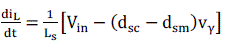 |
| Where Vin is the input voltage, iL is the input current, and vγ is the terminal voltage of the stacked Cockcroft Walton voltage multiplier. In the proposed converter switches Sc1 and Sc2 are used to generate an alternating supply to feed into the CW voltage multiplier and switches Sm1 and Sm2 are used to control the inductor energy to obtain a boost performance. |
| The diodes and capacitors are connected in cascaded connection to form a voltage multiplier. This is connected to the switches with a source and to parallel inductors. These form a two loop with two switches at both sides with a common inductor to boost the initial supply or source. The parallel inductors have mutual inductance due to which it helps in reducing the sudden increase in the output value. Here a capacitor is connected across a switch and the source. This will increase the system efficiency and increase the initial supply voltage to a certain amount. The Cockcroft Walton voltage multiplier is formed and another cascaded voltage multiplier is stacked to it and the output is taken from the D6cathode and D12 anode. The converter operates in continuous conduction mode, so the switch stresses, the switching losses, and EMI noise can be reduced as well. |
| The stacked Cockcroft Walton voltage multiplier is provided by a sinusoidal ac source with line frequency is used to analyse the behaviour of the stacked CW circuit through simulation using Fig.4. One inductor is connected between the ac source and the stacked CW voltage multiplier for smoothing the current iγ. During positive half cycle, that only one of the even diodes is conducted with the sequence D6-D4-D2, D12-D10-D8 and with the aim of the even and odd capacitors are charged discharged through the conducting diodes. Similar behaviour occurs during the negative half cycle, while the odd diodes are conducted with the sequence D5-D3-D1, D11-D9-D7 and the odd and even capacitors are charged and discharged. |
| The DC voltage gives the required initial voltage for the circuit to operate; the inductor stores the energy and boosts the voltage and this voltage has to be passed through the switches. The IGBT switches starts to operate as soon as it gets the gate pulse from the pulse generator and due to the varying in operation for individual IGBT the output gets increased slightly. Thus this part produces a voltage little higher than the input voltage. The parallel inductor helps in reducing the sudden rise of voltage at output side during the initial stage of the system. The capacitor connected across to the source and the switch increases the output and the system efficiency. |
| This voltage is given to the stacked voltage multiplier; the voltage multiplier multiplies the give voltage to certain times according to the number of stages used in the circuit. Then the output voltage is given to load after filtering it with a capacitive filter. The output voltage is taken as feedback and compared with a reference voltage and the resultant value is given to a PI controller and the pulse generation for the IGBT switches is automatically adjusted and the reference value can be set according to the load or according to the requirement. The desired output is obtained without any ripples and distortion with improved output voltage, thus a high voltage is obtained using a low voltage source. |
IV.SIMULATION & EXPERIMENTAL RESULTS
|
| The conventional converter is compared to the proposed converter by producing the output by both converters. Both the converters are simulated with and without load, when the load is applied the conventional converter showed more distortion in the output and the output voltage of the converter too got reduced but the proposed converter removed those distortion and produced a distortion free output and the output voltage too increased and maintained at a certain level. |
A.Comparison of Proposed Output with Conventional Converter Output
|
| When the nonlinear load is applied to the conventional converter Fig.5 the ripples obtained are too high and the distortion is too high, it produces nearly 310v, but the simulation output of the proposed converter Fig.6 shows that it does not have too much ripples and distortion when a nonlinear load is applied and it also obtains a voltage of 610v approximately. |
V. RESULT AND DISCUSSION
|
| The comparison chart of existing and proposed system output voltages is shown in Fig.7. The table 1 is the comparison table of output voltage of proposed and existing system. |
| The Comparison gives us a clear idea about the proposed converter which can produce large output without too much distortion, ripples and much more efficient than the conventional converter. This is obtained due to the addition of capacitor and the stacking of the circuit resulted in increase of voltage and the inductor and capacitor acts as a filter and produces a stable output. Thus the analysis of both converters shows that the proposed converter is more efficient and can be used in all fields. |
VI.CONCLUSION
|
| In this paper the operation of the Improved Transformerless high step-up dc–dc converter using stacked Cockcroft Walton voltage multiplier is explained, the design of the converter was discussed, and experimental results obtained. The proposed converter can produce a high output voltage with a low input voltage. The main advantage of this paper is that it increases the given input voltage by multiplying it without any use of transformer but just with the few switches, diodes and capacitor. The ripples, distortion present in the output voltage have been reduced and a high output voltage is obtained with a low input voltage. Here the use of the Stacked Cascaded Voltage Multiplier increases the output voltage and the parallel capacitor to the switch increases the efficiency and helps in increases the voltage too. The proposed converter can be applied to various applications like renewable energy, fuel cells, hybrid vehicle. The performance of the proposed converter is analysed using MATLAB. The Comparison gives us a clear idea about the proposed converter which is can produce large output without too much distortion, ripples and much more efficient than the conventional converter. |
| |
Tables at a glance
|
 |
| Table 1 |
|
Figures at a glance
|
 |
 |
 |
 |
| Figure 1 |
Figure 2 |
Figure 3 |
Figure 4 |
 |
 |
 |
| Figure 5 |
Figure 6 |
Figure 7 |
|
| |
References
|
- B. K. Bose (2000), “Energy, environment, and advances in power electronics,” IEEE Trans. Power Electron., vol. 15, no. 4, pp. 688–701.
- F. Blaabjerg, Z. Chen, and S. B. Kjaer (2004), “Power electronics as efficient interface in dispersed power generation systems,” IEEE Trans.Power Electron., vol. 19, no. 5, pp. 1184–1194.
- Q. Li and P. Wolfs (2008), “A review of the single phase photovoltaic module integrated converter topologies with three different dc link
- W. Li and X. He (2011), “Review of non-isolated high-step-up dc/dc converters in photovoltaic grid-connected applications,” IEEE Trans.Ind. Electron., vol. 58, no. 4, pp. 1239–1250.
- M. W. Ellis, M. R. Von Spakovsky, and D. J. Nelson (2001), “Fuel cell systems: Efficient, flexible energy conversion for the 21st century,”Proc. IEEE, vol. 89, no. 12, pp. 1808–1817.
- G. R. Walker and P. C. Sernia (2004), “Cascaded dc-dc converter connection of photovoltaic modules,” IEEE Trans. Power Electron., vol. 19,no. 4, pp. 1130–1139.
- J. Wang, F. Z. Peng, J. Anderson, A. Joseph, and R. Buffenbarger (2004), “Low cost fuel cell converter system for residential power
- L. S. Yang, T. J. Liang, and J. F. Chen (2009), “Transformerless dc-dc converters with high step-up voltage gain,” IEEE Trans. Ind. Electron.,vol. 56, no. 8, pp. 3144–3152.
- N. Mohan, T. M. Undeland, and W. P. Robbins (1995), Power Electronics, 2nded. New York: Wiley, pp. 172–178.
- A. L. Rabello, M. A. Co, D. S. L. Simonetti, and J. L. F. Vieira (1997), “An isolated dc-dc boost converter using two cascade control loops,”in Proc.IEEE ISIE, vol. 2, pp. 452–456.
|