Keywords
|
| Inductive coupling, Gate Drive Transformer, Astable multivibrator, MOSFET Driver, MOSFET Inverter Bridge. |
I. INTRODUCTION
|
| A recent trend in power supply design is the development of charging systems that are capable of wireless power transfer. This means that the power supply is not plugged into the device being charged. Wireless power transfer allows a convenient, easy to use battery charging of mobile phones and other mobile devices. No hassle with cables and plugs, just place the device on a pad and that’s it. Such a system even has the potential to become a standard charging solution. The ‘Inductive Charging Pad’, is a wireless power transfer system using inductive coupling. The system uses coupled magnetic fields to transfer electromagnetic energy from a charging base to receiver in a portable device. |
| The charging base circuit comprises of two parts, the device-side and the charger-side sub circuits. The charger-side consists of a power supply unit with an appropriate converter and a transmission coil while the device-side is made up of an inductive pick-up unit and a regulator. An output voltage and current level compatible to a Li Ion rechargeable battery is obtained at the regulator output terminal. |
| Improving the efficiency and the time rate of inductive charging to values comparable to the conventional chargers is the main objective of this project. |
II. TECHNOLOGY REVIEW
|
| Wireless charging is an emerging trend for mobile and portable devices with various products appearing in the market by providing significant user convenience. Magnetic resonance based charging is a technique that provides support for charging multiple receivers with the same transmitter. Wireless charging has been popular since 2009 with products like Palm Pre., Dell Latitude, PowerMat and many other similar products. The technologies for wireless charging can be either magnetic induction or radio frequency or optical or conduction. Magnetic induction converts electrical energy to magnetic energy. It allows transmission over an air gap and is typically short to midrange. For microwave or radio frequency, the parabolic dish focuses radio waves which are typically long range waves towards intended target. They can also includelow power receivers for energy harvesting. For optical or infrared, the laser light is focused on photovoltaic cells that convert light energy to power. In conduction, the power transfer occurs due to metallic contact between transmitter and receiver. Compared to inductive coupling and RF radiation, wireless power transfer via strong coupled resonance is more suitable for wireless power transfer in a range from a few centimeters to a few meters for mobile consumer devices. Magnetic resonance coupling is more advantageous since it has an extended range, alignment insensitivity and potential to support multiple receivers. |
III. PRINCIPLE OF OPERATION
|
| Inductive charging works on the principle of transformer. A transformer is a device that transfers electrical energy from one circuit to another through inductively coupled conductors the transformer's coils. A varying current in the first or primary winding creates a varying magnetic flux in the transformer's core and thus a varying magnetic field through the secondarywinding. This varying magnetic field induces a varying electromotive force (EMF) or "voltage", in the secondary winding. This effect is called mutual induction |
IV. BLOCK DIAGRAM
|
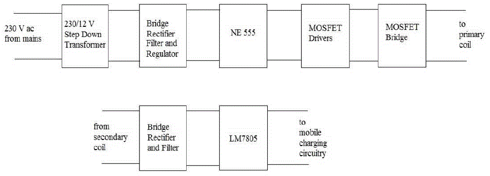
| The block diagram shown in Fig. 1 explains our approach to the design of the Inductive Charging set. A 230/12 V step down transformer is used the output of which is a sinusoidally varying voltage of 12 V amplitude. This 12 V ac voltage is then rectified, filtered and regulated to 12 V dc which is the power requirement to operate the 555 timer IC. The NE555 is made to act as an astable multivibrator to give square pulses of kHz frequency range. |
| The output square pulse of the NE555 is used to operate two MOSFET drivers which then drives the MOSFET Bridge. The primary coil of the Inductive coupling is connected to the output of MOSFET Bridge. When placed in alignment with the Primary coil and at a separation of a few millimeters, an alternating voltage is induced in the Secondary coil of the Inductive coupling. The voltage thus obtained at the secondary is rectified, filtered and regulated and is used to charge the handheld mobile device. |
V. SCHEMATICS
|
A. POWER SUPPLY
|
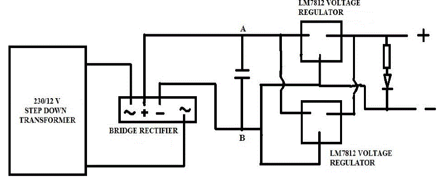
| The basic function of the power supply circuit is to obtain from the 230 V ac mains, a dc voltage of 12 V which is the required voltage level to operate the 8 pin NE555 IC. In order to do this the 230 V ac from mains is first stepped down to 12 V ac by using a 230/12-0-12 V step down transformer with a secondary current rating of 5A. |
| To rectify this 12 V ac, a BR68 single unit bridge rectifier is used. The single unit bridge rectifier is used so that the circuit is less bulky and also because the rectifier needed to have a current rating of 5 A. The 12 V dc output from BR68 is filtered using a 2200 micro farad radial capacitor. LM7812 voltage regulators are used to obtain proper dc voltage level of 12 V. Two LM7812 regulators in parallel is provided so that the current gets reduced when it branches into these two paths and does not damage the LM7812. This 12 V dc is used to operate the IC’s. The block schematics of a power supply module is shown in Fig. 2 |
B. 555 TIMERS AND MOSFET BRIIDGES
|
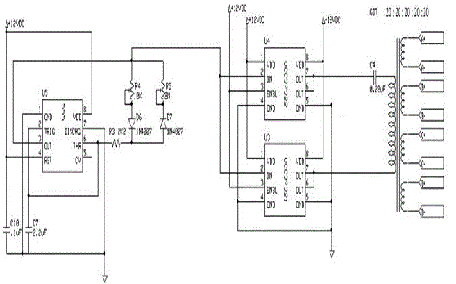
| The NE555 is operated from the 12 V dc of the power supply circuit. It operates as an astable multivibrator which gives a square pulse in the kHz frequency range. The 2.2 micro farad capacitor and the 10 k pot resistors that we used allowed us to vary the frequency from 1 to 3 kHz. The square pulse output of the NE555 is given to the input pins of IC’s UCC37322 and UCC37321 which are MOSFET drivers. MOSFET drivers are required here because the output of the NE555 if given directly to the gate terminals of the MOSFETs might not have been enough to drive the MOSFETs. The drivers UCC37322 and UCC 37321 act as a pair. If the pulse to the input pins of both are high, one IC of this pair is switched ON while the other is off, i.e., the current at the output of the drivers flow in one particular direction accordingly inducing a particular polarity in the primary of the Gate Driving Transformer(GDT). Fig. 3 shows the circuit diagram of 555 timer and the Gate Drive Transformer. |
| On the other hand, if the pulse to the input pins of both the driver IC’s is low, the driver IC which was earlier ON is switched OFF and the other is switched on. Consequently the current at the output of the drivers flow in the opposite direction and opposite polarity is induced in the primary of GDT. |
C. MOSFET BRIDGE
|
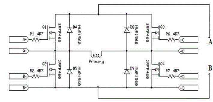
| The MOSFET Bridge in the circuit above acts as an inverter. The supply to the inverter from points A and B in the power supply circuit. According to the polarity induced in the primary of the GDT, in either case only two of the MOSFETs in the bridge conducts allowing an alternating current to pass through the primary coil of the inductive coupling. The significance of the GDT lies in the fact that the four output coils of the GDT are used to independently drive the four MOSFETs in the bridge. IRFP 460 power MOSFETs were used. Heat sinks had to be provided since MOSFETs of high current ratings were used. Diodes are provided across the drain and source of each MOSFET for its protection from current spikes. Fig. 4 shows the circuit diagram of MOSFET bridge circuit. It also shows the primary coil to which the output of the bridge is given. |
D. SECONDARY SIDE CIRCUIT
|
| The secondary coil if placed in alignment with the primary and at a separation of millimeter range, an ac voltage gets induced in it. A single unit bridge rectifier, W10 of 1 A current rating is used to rectify the voltage obtained at the secondary. A micro farad capacitor is used as a filter. Then the LM7805 regulator provided after the filter regulates the voltage and provides the proper voltage level of 5 V required to charge the Li ion batteries of handheld mobile devices. 5 V, 500 mA is the widely used charging specifications for Li ion batteries. Fig. 5 shows the design of the secondary circuit that is to be connected to the handset placed for charging. |
VI. GATE DRIVE TRANSFORMER
|
| Gate drive transformers simply deliver a voltage pulse or a series of voltage pulses to a semiconductor gate electronic circuits. Utilized in many gated semiconductor devices such as ordinary transistors, field effect transistors, |
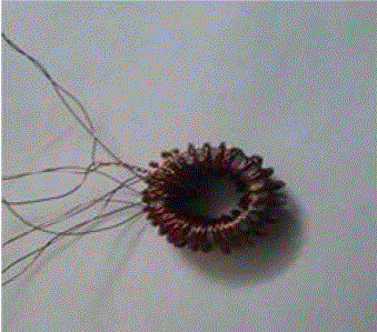
| and S.C.R.s and others. A gate drive transformer functioning in this manner could also be called a pulse transformer. A signal must be supplied to (or removed from) the device’s gate node to activate (or deactivate) the device. Some applications require a close reproduction of the pulse.Unity turns ratio (Turns ratio, 20: 20: 20: 20: 20) used to minimize leakage inductance and optimize coupling coefficient. Used in applications requiring isolation between the low level logic and high power output. When used, gate drive transformers are located within the circuitry driving the gate. Gate drive transformers are used to modify the voltage level to the gate, provide impedance matching, and to provide voltage isolation. If the gate drive transformer’s pulse initiates some action or event, the gate drive transformer could be called a trigger transformer.Fig. 6 shows the GDT designed for our purpose with a turns ratio of 20:20:20:20:20. It has 1 input coil and 4 output coils to independently feed the 4 MOSFET bridges. |
VII. INDUCTIVE COUPLING
|
| The pickup is inductively coupled to the transmission coils, meaning that the hand-wound inductive pickup coil is positioned close to and aligned with the transmission coil. Then the magnetic field produced by the transmitter passes through the dense loop of wires, inducing an electrical current. A single layer coil has two advantages. |
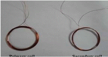
| Firstly, like all air core coils, it is free from iron losses and the non-linearity mentioned above.Secondly, single layer coils have the additional advantage of low self-capacitance and thus high significant frequency.These coils are mostly used above about 3 MHz. The transmitter and receiver side coils having 15 turns and 20 turns respectively and both of them made up of air cored planar coils off 5 cm diameter with 28 gauges magnet wires. Fig. 7 shows the primary and secondary coils which were hand wound and employed in the circuit. |
VIII. SIMULATION AND RESULT
|
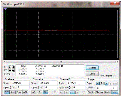
| The simulation of the circuit was done using ‘Multisim’ and the output obtained from the graph of the simulation clearly indicates that the output acquired is satisfactory for the intended purpose, i.e., the charging of mobile device. Hence the project was put to the next stage and the circuit realised. |
| Inductive charging system was successfully designed and implemented as specified in our proposal. The efficiency is calculated as the ratio of the power absorbed by the inductive pickup block on the target device to the power consumed by the power transmission block on the charger base. The output obtained with various turns ratio have been tabulated below. |
| Since the ratio of 15:20 gave the voltage sufficient to charge the mobile device that turns ratio was chosen for employing in the primary and the secondary coils. The coils were hand wound with 5 cm diameter using 28 gauge wire. |
IX. CONCLUSION
|
| Inductive charging carries a far lower risk of electrical shock, when compared with conductive charging, because there are no exposed conductors. |
| The main disadvantages of inductive charging are its lower efficiency and increased resistive heating in comparison to direct contact. Implementations using lower frequencies or older drive technologies charge more slowly and generate heat for most portable electronics. Inductive charging also requires drive electronics and coils that increase manufacturing complexity and cost. |
| The most needed improvements are to the inductive coils (to improve the efficiency) and implementing RFID (for wireless data transfer and automatic device sensing). |
| Automatic wireless charging of mobile electronics (phones, laptops, game controllers, etc.) in home, car, office, Wi-Fi hotspot while devices are in use and mobile. Direct wireless powering of desktop PC peripherals: wireless mouse, keyboard, printer, speakers, display eliminating disposable batteries and awkward cabling. There are some industrial applications such as Direct wireless power and communication interconnections across rotating and moving joints (robots, packaging machinery, assembly machinery, machine tools) eliminating costly and failure-prone wiring. Wireless electricity is a recently developed application of inductive charging. It has been demonstrated that it is feasible to transmit a significant amount of power at a high efficiency. |
ACKNOWLEDGEMENT
|
| We extend our sincere thanks to Prof. Radhakrishnan K, Head of the department for providing us with the guidance and facilities for the project. We also express our sincere gratitude to project coordinator Prof. Elizabeth Sebastian for their cooperation and guidance for preparing and presenting this project. We also extend our sincere thanks to all other faculty members of Electrical and Electronics Department and our friends for their support and encouragement. |
| |
Tables at a glance
|
 |
| Table 1 |
|
| |
Figures at a glance
|
 |
 |
 |
 |
| Figure 1 |
Figure 2 |
Figure 3 |
Figure 4 |
 |
 |
 |
 |
| Figure 5 |
Figure 6 |
Figure 7 |
Figure 8 |
|
| |
References
|
- Jonsenser Zhao,“A new calculation for designing multilayer planar spiral inductors”, July29,2010, pp 37-40.K. M. Passino, “Biomimicry ofbacterial foraging for distributed optimization,” IEEE Control Systems Magazine, vol. 22, no. 3, pp. 52-67, 2002.
- Benjamin H. Waters, Student Member IEEE, Alanson P. Sample, Student Member IEEE, PramodBonde, Member IEEE, and Joshua R. Smith,Member IEEE “Powering a Ventricular Assist Device (VAD) With the Free-Range Resonant Electrical Energy Delivery (FREE-D) System”,Proceedings of the IEEE , Vol. 100, No. 1, January 2012pp 138-149.
- Mehdi Kiani, Student Member, IEEE, Uei-Ming Jow, Student Member, IEEE, and MaysamGhovanloo, Senior Member, IEEE “Design andOptimization of a 3-Coil Inductive Link for Efficient Wireless Power Transmission”, IEEE Transactions On Biomedical Circuits And Systems,Vol. 5, No. 6, December 2011, pp 579-591.
- NehaChawla,SabriTosunoglu, Department of Mechanical and Materials Engineering, Florida International University, Miami, Florida, USA“State of the Art in Inductive Charging for Electronic Appliances and its Future in Transportation”, 2012 Florida Conference on RecentAdvances in Robotics, Boca Raton, Florida, May 10-11, 2012, pp 1-7.
- BasharatNizam, K L University “Inductive Charging Technique”, International Journal of Engineering Trends and Technology (IJETT),Volume4, Issue4, April 2013, ISSN: 2231-5381http://www.ijettjournal.org pp1054-1059.
- Hao Leo Li, Aiguo Patrick Hu, Senior Member, IEEE, and Grant Anthony Covic, Senior Member, IEEE, “A Direct AC–AC Converter forInductive Power-Transfer Systems”, IEEE Transactions On Power Electronics, Vol. 27, No. 2, February 2012, pp 661-668
- Sunderarajan S Mohan, Maria del Mar Hershenson, Stephen P Boyd, and Thomas H Lee, “Simple Accurate Expressions for Planar SpiralInductances”, IEEE journal of solid-state circuits, Vol. 34, No. 10, October 1999.
|