Keywords
|
| Traffic signal control system, microcontroller, vehicle detection, vehicle counting, Matlab. |
I. INTRODUCTION
|
| As the number of road users constantly increases, and resources provided by current infrastructures are limited, intelligent control of traffic will become a very important issue in the future. However, some limitations to the usage of intelligent traffic control exist. Avoiding traffic Jams for example are thought to be beneficial to both environment and economy, but improved traffic flow may also lead to an increase in demand [1]. There are several models for traffic simulation; we focus on optimization of traffic light controller in a city using image processing. The traffic control system based on vehicle density calculation tries to reduce possibilities of traffic jams, caused by traffic lights, to an extent. The system contains camera and microcontroller to process image for traffic density measurement which are mounted on roads respectively. Microcontroller controls the image processor system and counts number of vehicles passing on road. Based on different vehicles count, the microcontroller takes decision and updates the traffic light delays as a result. The traffic light is situated at a certain distance from the camera system. Thus based on vehicle count, microcontroller defines different ranges for traffic light delays and updates those accordingly.[2]the algorithm is Background extraction & Analysis (PCA) involves a image processing procedure that extracts the background from the image with objects and uses the extracted background image as a reference against images with objects.Theoretical developed, BEA is used for finding the most appropriate background image model to identify an object by extracting the most relevant information contained in the reference image.In this paper the objects that are refered to are vehicles |
II. HARDWARE
|
| The ARM Architecture is a 32-bit RISC processor developed by ARM limited that is widely used in a number of Embedded system .Because of their power saving features, ARM cpu’s are dominant where low power consumption is a critical design goal. There are 37 pieces of 32-bit registers.it is pipelined. ARM has three stages pipelining fetch, decode, execute .there are seven modes of operation. The ARM architecture is based on Reduced Instruction Set Computer (RISC) principles. The RISC instruction set and related decode mechanism are much simpler than those of Complex Instruction Set Computer (CISC) designs Reduced Instruction Set Computer has simple instruction. There is no need for microcode. It executes instruction faster. It has high performance. The Advantages of ARM architecture is high instruction throughput, low power consumption, Excellent real-time interrupt response, high performance. it is a small processor macro cell and it is cost effective. ARM Limited has incorporated a novel mechanism, called the Thumb architecture.[3-5] The Thumb instruction set is a 16-bit compressed form of the original 32-bit ARM instruction set, and employs dynamic decompression hardware in the instruction pipeline ARM cores are simple compared to most other general-purpose processors. A typical ARM chip contains several peripheral controllers, a DSP and some amount of on-chip memory. ARM ISA and pipeline designs are aimed to minimizing energy consumption. ARM architecture is highly modular: the only mandatory component of an ARM processor is the integer pipeline. All other components, including caches, MMU, FP unit and other co-processors are optional. |
III. PROTOTYPE COMPONENTS
|
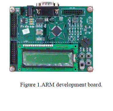
| The prototype consists of several components such as the ARM development board, traffic signal, camera, sensors. The arm development board consists of LPC2148 microcontroller which plays a major role. The traffic signal has a junction with the necessary component |
a. Serial communication
|
| It is the way that enables the different equipments to communicate to the outside world. It is called Serial because the data bits will be sent in a serial way over a single line |
b. MAX232
|
| It is an integrated circuit that converts signals from an RS-232 serial port to signals suitable for use in TTL compatible digital logic circuits. Register for serial communication is SCON-Serial Control Register. Baud rates can be set by using Timer-1(T1) only. Register corresponding to baud rate setting using timer-1 |
c. Baud Rate
|
| It is the Oscillator Frequency/384*(256-TH1). |
| d. ARM Processors. |
| The recent ARM processors have a 16-bit instruction mode, called Thumb. This is intended to allow smaller code where possible. T (Thumb)-extension shrinks the ARM instruction set to 16-bit word length, saving about 35-40% in amount of memory compared to 32.bit instruction set. For this extension a special decoder, with Thumb instructions decompressor and multiplexers, is used in the processors pipeline. |
| It is used For Low-Cost High Volume Application with Embedded Flash and SRAM, On-board AMBA-bus Peripherals (Advanced Microcontroller Bus Architecture) It is a Real-Time Deterministic behavior (no Cache required, Full Debug, Real-time Monitoring. |
| The LPC2148 microcontroller is based on a 16-bit/32-bit ARM7TDMI-S CPU with real-time emulation and embedded trace support that combine microcontroller with embedded high-speed flash memory of 512 KB. A 128-bit wide memory interface and unique accelerator architecture enable 32-bit code execution at the maximum clock rate. For critical code size applications, the alternative 16-bit Thumb mode reduces code by more than 30 % with minimal performance penalty. Due to their tiny size and low power consumption, LPC2148 microcontroller is ideal for applications where miniaturization is a key requirement, such as access control and point-of-sale. Serial communications interfaces ranging from a USB 2.0 Full-speed device, multiple UARTs, SPI, SSP to I2C-bus and onchip SRAM of 40 kB, make these devices very well suited for communication gateways and protocol converters, soft modems, voice recognition and low end imaging, providing both large buffer size and high processing power. Various 32-bit timers, single or dual 10-bit ADC(s), 10-bit DAC, PWM channels and 45 fast GPIO lines with up to nine edge or level sensitive external interrupt pins make these microcontrollers suitable for industrial control and medical systems. |
e. The Architecture of LPC2148
|
| Pipeline techniques are employed so that all parts of the processing and memory systems operate continuously. Typically, while one instruction is being executed, its successor is being decoded, and a third instruction is being fetched from memory. |
| The ARM7TDMI-S processor also employs a unique architectural strategy known as Thumb, which makes it ideally suited to high-volume applications with memory restrictions, or applications where code density is an issue. The key idea behind Thumb is that of a super-reduced instruction set. Essentially, the ARM7TDMI-S processor has two instruction sets: The standard 32-bit ARM set.,A 16-bit Thumb set. |
f. On-Chip Flash Memory
|
| The LPC2148 incorporate 512 kB flash memory system respectively. This memory may be used for both code and data storage. Programming of the flash memory may be accomplished in several ways. It may be programmed In System via the serial port. The application program may also erase and/or program the flash while the application is running, allowing a great degree of flexibility for data storage field firmware upgrades, etc. Due to the architectural solution chosen for an on-chip boot loader, flash memory available for user’s code on 500 kB. The LPC2148 flash memory provides a minimum of 100000 erase/write cycles and 20 years of data-retention. |
g. On-chip Static RAM:
|
| On-chip static RAM may be used for code and/or data storage. The SRAM may be accessed as 8-bit, 16-bit, and 32- bit. The LPC2148 provide 32 kB of static RAM. Also an 8 kB SRAM block intended to be utilized mainly by the USB can also be used as a general purpose RAM for data storage and code storage and execution. |
h. General purpose parallel I/O (GPIO):
|
| Device pins that are not connected to a specific peripheral function are controlled by the GPIO registers. Pins may be dynamically configured as inputs or outputs. Separate registers allow setting or clearing any number of outputs simultaneously. The value of the output register may be read back, as well as the current state of the port pins. LPC2141/42/44/46/48 introduce accelerated GPIO functions over prior LPC2000 devices: |
i.UARTs
|
| The LPC2148 contains two UARTs. In addition to standard transmit and receive data lines, the LPC2148 UART1 also provides a full modem control handshake interface. Compared to previous LPC2000 microcontrollers, UARTs in LPC2148 introduce a fractional baud rate generator for both UARTs, enabling these microcontrollers to achieve standard baud rates such as 115200 with any crystal frequency above 2 MHz In addition, auto-CTS/RTS flow-control functions are fully implemented in hardware (UART1). |
j. 10-bit ADC
|
| The LPC2148 contains two analog to digital converters. These converters are single 10-bit successive approximation analog to digital converters. While ADC0 has six channels, ADC1 has eight channels. Therefore, total number of available ADC inputs for is 14. |
k. 10-bit DAC:
|
| The DAC enables the LPC2148 to generate a variable analog output. The maximum DAC output VREF voltage |
l.. USB 2.0 device controller
|
| The USB is a 4-wire serial bus that supports communication between a host and a number (127 max) of peripherals. |
m. Pulse width modulator:
|
| The PWM is based on the standard timer block and inherits all of its features, although only the PWM function is pinned out on the LPC2148. The timer is designed to count cycles of the peripheral clock (PCLK) and optionally generate interrupts or perform other actions when specified timer values occur, based on seven match registers. The PWM function is also based on match register events. |
n. Crystal oscillator:
|
| On-chip integrated oscillator operates with external crystal in range of 1 MHz to 25 MHz The oscillator output frequency is called fosc and the ARM processor clock frequency is referred to as CCLK for purposes of rate equations, etc. fosc and CCLK are the same value unless the PLL is running and connected. o. PLL: |
| The PLL accepts an input clock frequency in the range of 10 MHz to 25 MHz The input frequency is multiplied up into the range of 10 MHz to 60 MHz with a Current Controlled Oscillator (CCO). The multiplier can be an integer value from 1 to 32 (in practice, the multiplier value cannot be higher than 6 on this family of microcontrollers due to the upper frequency limit of the CPU). The CCO operates in the range of 156 MHz to 320 MHz, so there is an additional divider in the loop to keep the CCO within its frequency range while the PLL is providing the desired output frequency. The output divider may be set to divide by 2, 4, 8, or 16 to produce the output clock. Since the minimum output divider value is 2, it is insured that the PLL output has a 50 % duty cycle. The PLL is turned off and bypassed following a chip reset and may be enabled by software. The program must configure and activate the PLL, wait for the PLL to Lock, then connect to the PLL as a clock source. The PLL settling time is 100 ms. Regulator is used to eliminate ripple by setting DC output to a fixed voltage. |
| p. Transformers |
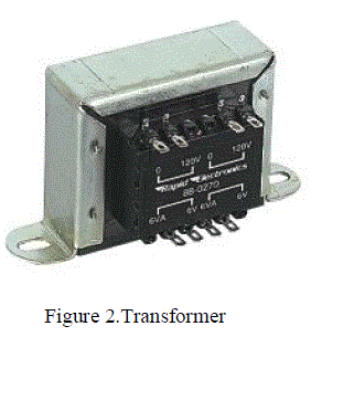
| They convert AC electricity from one voltage to another with little loss of power. Transformers work only with AC and this is one of the reasons why mains electricity is AC. Step-up transformers increase voltage, step-down transformers reduce voltage. Most power supplies use a step-down transformer to reduce the dangerously high mains voltage (230V in UK) to a safer low voltage. Transformers increase voltage, step-down transformers reduce voltage. Most power supplies use a step-down transformer to reduce the dangerously high mains voltage (230V in UK) to a safer low voltage. |
. p.Regulator:
|
| Voltage regulators ICs are available with fixed (typically 5, 12 and 15V) or variable output voltages. They are also rated by the maximum current they can pass. Negative voltage regulators are available, mainly for use in dual supplies. Most regulators include some automatic protection from excessive current ('overload protection') and overheating ('thermal protection'). Many of the fixed voltage regulator ICs have 3 leads and look like power transistors, such as the 7805 +5V 1A regulator shown on the right. They include a hole for attaching a heat-sink if needed |
IV. ALGORITHM,EXPERIMENT, SIMULATION AND RESULT
|
A.Algorithm
|
| Background extraction & Analysis (PCA) involves a image processing procedure that extracts the background from the image with objects and uses the extracted background image as a reference against images with objects.Theoretical developed, BEA is used for finding the most appropriate background image model to identify an object by extracting the most relevant informatiocontained in the reference image.In this paper the objects that are refered to are vehicles |
B. Prototype Implementation
|
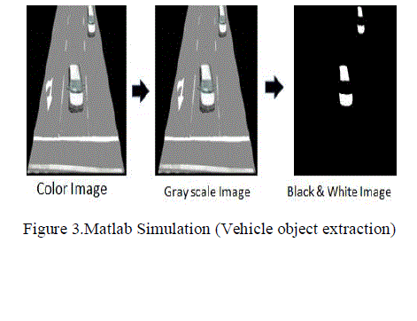
| Broadly speaking, the architecture of a traffic signal control system can be divided into three major component as in Figure 2. The first component is the video camera sensor. It captures the images of traffic condition at every intersection of each lane. Decision is made by the traffic light engine depending on the density of traffic. The next component is the traffic engine. After the first component gave the data in the form of image, this component will process the image to determine the number of vehicles in each lane intersection. This data will be counted with the Fuzzy constraint satisfaction methodology (FCM) which gives the best time for traffic signal. At the early stage, we use Beagle Board with ARM Cortex-A8.At the later stage of the experiment we use ARM7TDMI-S LPC2148 with specification 512KB internal flash 32KB shared sram [6]. The result of the calculation which is generated but traffic engine is sent to the traffic signal. The traffic engine will traffic signals corresponding to the data received. we use a microcontroller LPC 2148 and a miniature of traffic signal. Microcontrollers are used to translate the result of the traffic engine that is ARM to digital signal which will be represented by the miniature of traffic signals .the LED’s glow according to the result of the traffic engine. The simulation is thus obtained from MATLAB. The program is flashed to the LPC2148 microcontroller which in turn processes the program and result in lighting of the traffic signal. The LED’s in the traffic signal glow according to the vehicles lined up in the intersection. It glows with the required time delay needed for the traffic at that particular moment.[7] The simulation result is it detects the number of Vehicles and the area of each vehicle. The unit of area is in pixels. The color image, gray scale image and the black and white image is given in matrix form. |
| The image conversion chart is shown in Figure 3.The color image is converted to the gray scale image, which is then converted to the black and white image. |
| 1. Background extraction: |
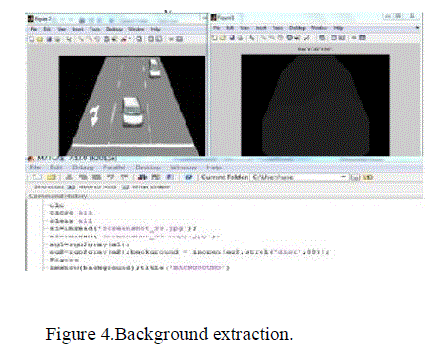
| In this method, the Background Image is doctored or extracted from Real time Image by background extraction codes |
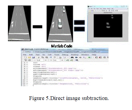
| 2. Direct Image subtraction: |
| In this type, a pre-captured background image of the road is used to compare with traffic mounted road image to detect and obtain number of vehicles . |
| The existing image is subtracted from the background image to give the desired output. |
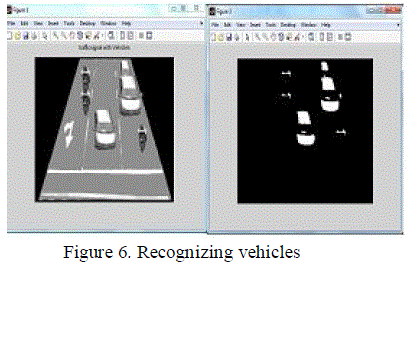
| Recognizing the elements of different features: |
| The elements of different structures are recognized and detected. The figure 6.shows the detected vehicles |
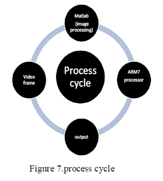
| The process cycle is given in Figure 7.The image is received from the video frame .It undergoes image processing technique and the result obtained is processed by the ARM processor. Finally the required output is obtained. |
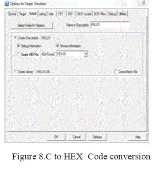
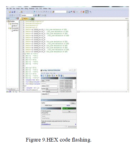
| The programming in ARM7 is done using the high level language. Any processor reads and writes only 1’s and 0’s.we write the program in C++ but the ARM understands only Hex code and therefore the code is converted into HEX code for the ARM to function. Using Hex code flash drivers, the Hex codes written into ARM7 program memory. |
V. CONCLUSION
|
| The method of vehicle detection and counting from a image has been implemented using matlab and ARM development board and LPC 2148 microcontroller. The accuracy of vehicle detection depends on the weather conditions. Further modification in the algorithm can improve the system accuracy. |
| |
Figures at a glance
|
 |
 |
 |
 |
 |
| Figure 1 |
Figure 2 |
Figure 3 |
Figure 4 |
Figure 5 |
 |
 |
 |
 |
| Figure 6 |
Figure 7 |
Figure 8 |
Figure 9 |
|
| |
References
|
- Traffic Management Centre. Last accessed on December, 2010
- Celil Oz Kurt, et al. “Automatic Traffic Density Estimation and Vehicle Classification For Traffic Surveillance Systems Using NeuralNetworks. Mathematical and Computational Applications”, Vol. 14, No. 3, pp. 187- 196, 2009.
- Ronan O’Malley. “Rear-Lamp Vehicle Detection and Tracking in Low- Exposure Color Video for Night Conditions”.IEEE Transactions on Intelligent Transportation Systems, Vol. 11, No. 2, June 2010
- WisnuJatmiko, et.al,” Detection and Counting of Vehicles Based on Video Processing In Distributed Traffic System”, International Conferenceon Advance Computer Science and Information System 2010.
- EhsanAzimirad, NaserPariz, and M. BagherNaghibi Sistani. “A Novel Fuzzy Model and Control of Single Intersection at Urban TrafficNetwork”. IEEE Systems Journal, VOL. 4, NO. 1, MARCH 2010.
- W. Jatmiko, et. al. Self-Organizing Urban Traffic Control Architecture With Swarm-Self Organizing Map In Jakarta: Signal Control System AndSimulator. “International Journal on Smart Sensing and Intelligent Systems” September 2010.
- Jatmiko, W., Hariyadi, F., Krisnadhi, A. A.,Takagawa, I., Sekiyama, K.,WisnuJatmiko, et.al,” Enhanced Distributed Traffic Control with Swarm-Self Organizing Map in Jakarta based on Traffic Signal Phasing”,International Conference on Advance Computer Science and Information System 2010.
|