Keywords
|
| Include Current Transformer (CT), KEIL & FLASH software, Microcontroller, optocoupler, PCC (Point of common coupling), Schottky diode, SPI (Serial Peripheral Interface) Communication, voltage divider. |
INTRODUCTION
|
| Basic instruments for the most accurate measurement of electric power and energy are digital electricity meters. They use digital multiplication of voltage and current samples, received from one A/D converter with multiplexed inputs, or they may use separate A/D converter for each input signal. The advantages of such instruments are obvious: high accuracy, short- and long-term stability, complex net parameters measurements, possibility of remote automated data processing, auto calibration, safest and many other functions resulting from the microprocessor-based digital system possibilities. With today„s high computing power of digital signal processors it is also simple to measure the reactive power, apparent power, phase shift, power factor and the frequency spectrum of the power network signals. Very important characteristic of electricity meters is their accuracy. It depends on the accuracy of the analogue input circuits, the accuracy of the sampling process itself, the accuracy of A/D conversion and the accuracy of digital calculations. In digital sampling electricity meters the measurement error can be simply eliminated in the digital signal processing. In this case the main problem is the stability of the parameters of these parts which handle the measured signals. The analogue input circuits must be constructed using highly stable components. There are many methods of error correction in digital electricity meters. Most of these methods use software correction based on calibration process. Digital electricity meters have different measurement and communication possibilities and different prices. The accuracy of the best instruments is of the order 0.01 %. |
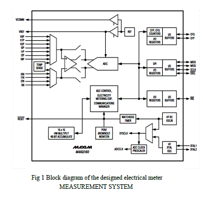
| The proposed instrument is able to measure all basic three-phase net parameters (rms values of voltages and currents, active, reactive and apparent power, power factor, frequency and energy delivered into the load). It can calculate the frequency spectra using FFT. Block diagram of the proposed instrument for power and energy measurement is shown in Fig.1. Analogue part contains circuits for sensing and conditioning of the net voltages and currents. The DSP part of MAXQ3183 makes necessary calculations and signal processing in digital form. It also contains software for three-phase signal generation with the output through a D/A converters block and a frequency output with the frequency proportional to the measured power. |
MEASUREMENT SYSTEM
|
| Microcontroller based energy meter is proposed .It has the ability that the utility company can monitor and control the power supply to its spatially distributed consumers. It has a master device that can isolate or resume the electricity supply to any of its customers with the capability of remote billing. This meter acts as a check meter to detect the meter tampering. In addition, metering systems can collect and process data, and can detect abnormalities in load profiles indicating electricity theft. |
REFERENCE DESIGN
|
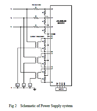
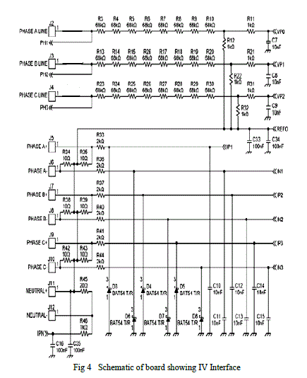
| The MAXQ3180 has three voltage channels, four current channels, and an internal channel for temperature measurement. The MAXQ3180 reference design uses resistor-dividers for voltage sensing and current transformers for current sensing. |
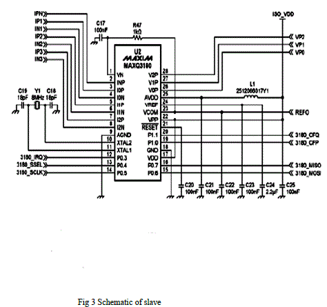
| Connection diagram for voltage and current sensing are shown in fig.2. Voltage of pins shown in fig3. for MAXQ3183 must not exceed as shown below: |
| Absolute Maximum Rating |
| Voltage Range on DVDD Relative to DGND .........-0.3V to +4.0V |
| Voltage Range on AVDD Relative to AGND..........-0.3V to +4.0V |
| Voltage Range on AGND Relative to DGND .........-0.3V to +0.3V |
| Voltage Range on AVDD Relative to DVDD ..........-0.3V to +0.3V |
| Voltage Range on Any Pin Relative to |
| DGND except VxP, IxN Pins..............................-0.3V to +4.0V |
VARIABLE DESCRIPTION
|
| VFS Voltage transducer value in volts. The AC-voltage input amplitude produces VREF/2 (~1.024V) volts on the voltage-input pins of the MAXQ3180. This MAXQ3180 reference design uses a voltage-divider consisting of 545kΩ (8 × 68 + 1) and 1kΩ, which gives a VFS = 545/1 × (2.048/2) = 558.08 ~ 558 (V). |
| IFS Current transducer ratio in amperes. It is the AC-current input amplitude that would produce VREF/2 (~1.02V) volts on the current-input pins of the MAXQ3180. This reference design uses a current transformer of primary/secondary ratio = 2500 and a burden resistor value of 660Ω. So itâÃâ¬ÃŸs IFS = 1.024 × 2500/660 = 3.857. ~ 4 (A). |
| VLSB LSB for virtual voltage registers in nV. VLSB = 1 means a value of 1 in the virtual voltage registers, so (V.X, X = A, B, C) represents 1nV. |
| ILSB LSB for virtual current registers in nA VLSB = 1 means a value of 1 in the virtual current registers, so (I.X, X = A, B, C) represents 1nA. |
| PLSB LSB for virtual power registers in nW, VLSB = 1 means a value of 1 in the virtual power registers, so (PWRP.X, PWRQ.X, PWRS.X, PWRPF.X, PWRQF.X, PWRSF.X, X = A, B, C) represents 1nW |
SPI COMMUNICATION
|
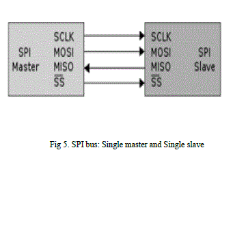
| The Serial Peripheral Interface Bus or SPI bus is a synchronous serial data link standard that operates in full duplex mode. Devices communicate in master/slave mode where the master device initiates the data frame. Multiple slave devices are allowed with individual slave select (chip select) lines. Sometimes SPI is called a "four-wire" serial bus, contrasting with three-, two-, and onewire serial buses. |
OPERATION
|
| The SPI bus can operate with a single master device and with one or more slave devices. If a single slave device is used, the SS pin may be fixed to logic low if the slave permits it. As, single slave is used in our hardware, so we made it logic low. To begin a communication, the master first configures the clock, using a frequency less than or equal to the maximum frequency the slave device supports. Such frequencies are commonly in the range of 1–70 MHz For proper communications operation, the SPI clock frequency used by the master must be less than or equal to the MAXQ3183âÃâ¬ÃŸs clock frequency divided by 4. For example, when the MAXQ3183 is running at 8MHz, the SPI clock frequency must be 2MHz or less. And if the MAXQ3183 is running in LOWPM Mode (or if the crystal is still warming up), the SPI clock frequency must remain at 250 kHz or less for proper communications operation. The master then pulls the slave select low for the desired chip. If a waiting period is required (such as for analog-to-digital conversion) then the master must wait for at least that period of time before starting to issue clock cycles. During each SPI clock cycle, a full duplex data transmission occurs: the master sends a bit on the MOSI line; the slave reads it from that same line the slave sends a bit on the MISO line; the master reads it from that same line |
| Not all transmissions require all four of these operations to be meaningful but they do happen. Transmissions normally involve two shift registers of some given word size, such as eight bits, one in the master and one in the slave; they are connected in a ring. Data is usually shifted out with the most significant bit first, while shifting a new least significant bit into the same register. After that register has been shifted out, the master and slave have exchanged register values. Then each device takes that value and does something with it, such as writing it to memory. If there is more data to exchange, the shift registers are loaded with new data and the process repeats. |
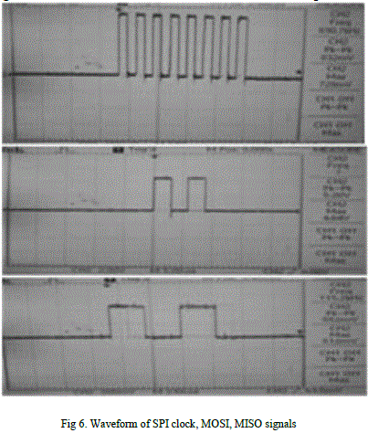
| In master mode, the SCLOCK pin is always an output and generates a burst of eight clocks whenever user code writes to the SPIDAT register. The SCLOCK bit rate is determined by SPR0 and SPR1 in SPICON. Also note that the SS pin is not used in master mode. If the parts need to assert the SS pin on an external slave device, a port digital output pin should be used. In master mode, a byte transmission or reception is initiated by a write to SPIDAT. Eight clock periods are generated via the SCLOCK pin and the SPIDAT byte being transmitted via MOSI. |
| With each SCLOCK period, a data bit is also sampled via MISO. After eight clocks, the transmitted byte will be completely transmitted, and the input byte will be waiting in the input shift register. The ISPI flag will be set automatically, and an interrupt will occur if enabled. The value in the shift register will be latched into SPIDAT |
Clock Polarity and Phase
|
| In addition to setting the clock frequency, the master must also configure the clock polarity and phase with respect to the data. For CPHA=0, data is captured on the clock's rising edge (low→high transition) and data is propagated on a falling edge (high→low clock transition). For CPHA=1, data is captured on the clock's falling edge and data is propagated on a rising edge. At CPOL=1 the base value of the clock is one (inversion of CPOL=0) For CPHA=0, data is captured on clock's falling edge and data is propagated on a rising edge. For CPHA=1, data is captured on clock's rising edge and data is propagated on a falling edge. That is, CPHA=0 means sample on the leading (first) clock edge, while CPHA=1 means sample on the trailing (second) clock edge, regardless of whether that clock edge is rising or falling. Note that with CPHA=0, the data must be stable for a half cycle before the first clock cycle. For all CPOL and CPHA modes, the initial clock value must be stable before the chip select line goes active. |
Read and Write Procedures
|
| Every defined register on the MAXQ3183 has a 12-bit address (from 0 to 4095). This address is used when addressing the register for either a read or write operation. Addresses 0 to 1023 (000h to 3FFh) are used to address RAM registers. Registers with addresses from 1024 to 4095 (400h to FFFh) are used for virtual registers and special command registers. Each command consists of a read/write command code, a data length (1, 2, 4, or 8 bytes), a 12-bit register address, and the specified number of data bytes followed optionally by a cyclic redundancy check (CRC). Since SPI is a full-duplex interface, the master and slave must both transmit the same number of bytes during the command. When a multiple-byte register is read or written (2/4/8 byte length), the least significant byte is read or written first in the command. Every transaction begins with the master sending 2 bytes that contain the command (read or write), the address to access, and the number of bytes to transfer. Every SPI peripheral must return 1 byte for every byte it receives. If the master is reading 1 or more bytes from the MAXQ3183, it must send dummy bytes during the cycles when it is receiving a multibyte response to a request, meeting the “send a byte to get a byte” requirement. But the MAXQ3183 could require time to calculate the result, and thus might not have it ready when the master sends the dummy byte. For this reason, the MAXQ3183 always sends zero or more bytes of a NAK character (0x4E or ASCII „NâÃâ¬ÃŸ) followed by an ACK character (0x41, or ASCII „AâÃâ¬ÃŸ) before sending the data. If the master is writing 1 or more bytes, it sends the data to be written immediately after sending the command. The MAXQ3183 returns ACK (0x41) for each data byte. It then returns NAK (0x4E) until the write cycle is complete, after which it returns a final ACK. |
Registers
|
| SPCR (SPI control register)/SPCTL Value: SPCTL=0x51 |
| SPCFG SPI Configuration register Address: 0xAAh Value : 0x00h |
| SPDAT SPI Data register Address: 0x86h |
| As the SPDAT register will get some value, SPI clock of 8 pulses will be generated by microcontroller. Details about these registers can be find in P89V51RD2 Microcontroller datasheet [1]. |
SERIAL COMMUNICATION
|
| Serial communication means data can be transmitted over single path using single pathway. This is employed for transmitting the data from one station to another. 300 baud rate is used for the data transmission and connected in following fashion. Following registers have been used for setting the baud rate and making the code for transmitting and receiving of the data: |
| ïÃâ÷ SCON: Address: 0x98H Value : 0x50H |
| ïÃâ÷ TMOD Value: 0x20H |
| Details about these registers can be seen in P89V51RD2 datasheet [1]. |
COMPONENT SELECTION AND SYSTEM DESIGN
|
| Basic system as discussed in the previously has used following components:- |
| (1) Microcontroller (P89V51RD2) |
| (2) Maxq3183 |
| (3) Sensors (Current Transformer CT1052) |
| (4) Opt coupler (6N137) |
| (5) Filter (RC Passive low pass Filter) |
| (6) Voltage Divider |
| (7) Schottky diode |
| (8) LCD |
| (9) RS232 driver |
| The current transducer ratio (ITR) = CT_N/ (2 x R) = 2000/ (2 x 10) =100 (A/V), IFS = 102.4A |
| The voltage transducer ratio (VTR) = (R1 + R2)/R2 = 545, VFS = 558.1V. |
| 16x2 LCD i.e. 16 words in a line with 2 line available to display data, is used to display the data receive by microcontroller from MAXQ3183. Pot (Variable resistor) is used to set the contrast voltage near 0.180V D.C. Port 0 of microcontroller is used for data transmission from microcontroller to LCD, while port2 is used as control pin. An RS-232 driver circuit was constructed to interface the modem to the host microcontrollerâÃâ¬ÃŸs serial port. The serial port uses +15V to represent a binary “1” and –15V to represent a binary “0”. The RS-232 driver circuit converts these voltages to and from the +5V and 0V binary representations suitable for the rest of the modem. The circuit is based on a dedicated IC, the MAXIM RS-232CPE line driver IC |
RESULTS
|
| SPI communication code for interfacing the microcontroller and MAXQ3183, energy metering chip, has been developed successfully in KEIL software which makes its hex file. This hex file is further burnt into microcontroller using Flash Programmer. This makes the energy meter for knowing the various parameter of the supply. These parameter are compared at the 2 points (such as Point of common coupling and load end or in power generating point and PCC) to estimate the theft successfully. Hardware is capable to measure the various parameters such as voltage, current, power etc and tell about the phase in which power theft happened by sending the data from load end to coupling end through serial communication and comparing its power. Maxq3183 reading is compared with the help of FLUKE power analyzer to estimate the error as shown below. |
CONCLUSION
|
| Microcontroller is interfaced with Maxim chip to form a meter. The analogue part of the instrument consists of the signal sensing and conditioning circuits for the three voltage and current channels. The digital part contains the microcontroller board with the connected keyboard, LCD display, serial interface to computer, the board for the necessary calculations and the separate voltage and current channels for every voltage and current signals. Modern Maxim MAXQ3183 was used to get a powerful measuring system. Error sources and error correction are briefly mentioned. Simple current and voltage calibration were done to overcome the errors in measurement. The resulting errors of simplified calculations are compared with the actual reading from power analyzer and show the accuracy of the order of tenth per cent. |
ACKNOWLEDGEMENT
|
| The setup was created at MHRD Lab at NIT kurukshetra setup by Dr. L M Saini. The authors would like to thank Dr. K S Sandhu, HOD, EED, NIT kurukshetra for providing the facility to make the arrangement for establishing this setup. |
Tables at a glance
|
 |
 |
 |
 |
| Table 1 |
Table 2 |
Table 3 |
Table 4 |
|
Figures at a glance
|
 |
 |
 |
| Figure 1 |
Figure 2 |
Figure 3 |
 |
 |
 |
| Figure 4 |
Figure 5 |
Figure 6 |
|
References
|
- Datasheets of MAXQ3183, P89v51rd2, CT1052, 6N137.
- Reference design for an energy meter using the MAXQ3180/MAXQ3183 AFE by Kennith Tang. Application note 4663.
- How to Use SPI on the MAXQ3180 Microcontroller. By Ben Smith. Application Note: 4246.
- Getting started with MAXQ3180: Configuring the registers. By Ben Smith. Application Note: 4642.
- AN836 Application note for Schottky diode.
- Book Named “8051 Microcontroller and Embedded system” by Mohammad Ali Mazidi.2nd Edition Year 2008-2009.
- Characteristics of power line channel and their effect on designing of communication system, published in international journal of Advance Engineering and Application, ArchanaAggarwal, R Singh, NelooferAfzal. Issue published in International journal of Advanced Engineering and Application. Pages 135-137, Jan2011
- Measurement of power in three phase circuit volume2 EE, Module 5, Lesson 20, and IIT Kharagpur.
- F. Leens, “An Introduction to I2C and SPI Protocols,” IEEE Instrumentation & Measurement Magazine, pp. 8-13, February 2009
- PranitaWani and A.S.Bhide , Design and implementation of ADC with microcontroller interfacing for data acquisition system, World Journal of Science and Technology 2012, 2(4):93-96
- Md. MejbaulHaque, Md. Kamal Hossain, Md Mortuza Ali, Md. Rafiqul Islam Sheikh, Microcontroller based Single Phase Digital Prepaid Energy Meter For Improved Metering and Billing System, International Journal of Power Electronics and Drive System (IJPEDS) Vol.1, No.2, December 2011, pp. 139~147
- Gaetano Pasini, Lorenzo Perreto, Elisa Pivello, Roberto Tinarelle, Performance Evaluation of a multifunctional Energy metering IC undersinusoidal and Non Sinusoidal conditions. Electric Power Quality and Utilization, Journal Vol.XIII, No. 1, 2007.
- IrfanQuazi,Sachin Kumar Gupta,Rajendra Prasad, Pre-paid Energy Meter based on AVR Microcontroller, International Journal of Engineering Research and Applications (IJERA), Vol. 1, Issue 4, pp.1879-1884
- Saptarshi De, Rahul Anand, A Naveen and SiratMoinuddin, “E-Metering Solution for checking energy thefts a streamlining revenuecollection in India”, Student Member, IEEE, 2003.
- Ashok Kumar Rajput, Simulation based measurement of three phase active, reactive and apparent power by two wattmeter methods with Labview, Indian journal of Engineering, vol3, no. 7, May 2013.
|