Multiphase dc-dc converters are widely used in modern power electronics applications due to their advantages over single-phase converters. Such advantages include reduced current stress in both the switching devices and passive elements, reduced output current ripple, increase in output voltage and overall efficiency and so on. The output current ripple of a converter can be significantly reduced by virtue of the interleaving connection. This paper presents a design and simulation of an interleaved high step up DC-DC converter with PID controller. The control strategy of the converter is based on a Proportional-Integral-Derivative (PID) controller. The proposed converter achieves a high step-up voltage-conversion ratio without extreme duty ratio and the numerous turns-ratios of a coupled inductor and reduction in the input current ripple with the efficiency higher than 97%.The PID controller is used in the feedback to reduce the rise time and steady state error. The proposed interleaved high step up DC-DC converter model along with PID controller is modeled using SIMULINK and the simulation results are presented in this paper to authenticate the proposed scheme.
Keywords |
| Interleaved boost, high step up DC-DC converter, PID controller. |
INTRODUCTION |
| Interleaved connection is a method in which the additional circuit is added in between the input and output of
the main circuit in order achieve the increase in overall efficiency and output voltage of the converter and also reduce
in input ripple and output ripple. |
| Interleaving is not a new technique earlier it was only used in the buck converter topology and there have been
many papers describing the use of multiphase buck converters, especially for high-performance high-power
applications [1, 2, and 3]. However, all the advantages of interleaving, such as higher efficiency, increase in output
voltage and reduced input and output ripple for voltage/current, are also realized in the boost topology. Most of the
controllers used in buck applications apply equally well when configured for use in an interleaved boost application. In
[4] multi-phase buck converter controlled by PID is presented. |
LITERATURE REVIEW |
| Now a day’s the interleaved high step up DC-DC converter has been widely used in photovoltaic generation, electric
vehicles and power factor correction due to its high power density and fast dynamic response [5]-[6]. The input current
ripple of the conventional boost converter is inversely proportional to its input inductor value [7], which means that a
large inductor value will result in low input current ripple; however, a large inductor value increases the total weight of
a capacitor with low ESR must be used [8]. Interleaved parallel structure has been applied in many high power density
applications [9]-[10] in order to minimize the input current ripple, reduce the passive component size, improve the
transient response and increase the power level. The frequency doubling characteristic of the interleaved structure can
significantly reduce the output capacitor value and the input current ripple of the converter, but the quality of input
power supply will still be deteriorated by the input current ripple especially in the large current applications [11].
Coupled inductor IBC proposed in [12]-[13] has used a coupled inductor to achieve the input current ripple
cancellation, and their applications can be found in [14]. However the leakage inductance of the coupled inductor
increases the current stress of the output diodes, introducing extra EMI problems. A soft switching circuit for IBC is
presented in [15]. It’s an attractive solution to avoid the major drawbacks of the coupled inductor; however, the control strategy of this circuit is too complex and not cost-effective on the other hand, since small inductor values increase the
loss of the capacitor of the converter. |
| These drawbacks can be overcome by the interleaved high step up DC-DC converter which consists of two
boost converters connected in interleaved structure to achieve high step-up voltage-conversion ratio without extreme
duty ratio and the numerous turns-ratios of a coupled inductor, reduction in the input current ripple with the higher
efficiency and reduction the rise time and steady state error. |
PROPOSED CONVERTER |
| The proposed converter is shown in Fig. 1. The proposed converter compromise of two boost converters
connected to each other in the form of interleaved structure and the PID controller in the feedback. |
| The proposed converter consists of a two coupled inductors T1 and T2 with the floating active switches S1, S2
.It has two primary windings N1, N3 of a coupled inductors T1, T2 both are similar to the input inductor of the
conventional boost converter, and the capacitors C1, C3 and diodes D1, D3 receives leakage inductor energy from N1
and N3. The secondary windings N2, N4 of coupled inductors T1 and T2 are connected with another pair of capacitors
C2, C4 and diode D2, D4 which are in series with N1 and N3 in order to further enlarge the boost voltage. The rectifier
diode D5 connects to its output capacitor C5. |
| Interleaved high step up DC-DC converter show in Fig 1 . Here it is two phase operations which mean it is
compromise of two boost converters. These boost converters have same parameter and operating principle which are
operating 180 degree out of phase. The input current is sum of two currents that is the input current is split up in two
paths I1 and I2.These two converters are operating at different phases. When the supply is turned on they will be
current ripple generated by the leakage inductors Lk1 and Lk3 but due to the two converters which are operating in
parallel stages at different phases, the input ripple currents iLk1 and ilk3 cancel each other and they is reduction in the
input ripple current that the boost inductor caused. Hence they will be increase in the overall efficiency compared to single boost converter. Here the both converters phases are combined at the output capacitor C5 so the output-capacitor
current is the sum of the two diode currents, Id2+Id4, minus the dc-output current Iout , which reduces the outputcapacitor
ripple, Icout .thus effective ripple frequency is doubled, making ripple voltage reduction much easier. And the
voltage across the output diode D5 is sum of two diode voltages Vd2+Vd4. |
| A PID controller show in FIG 1 is a generic control loop feedback mechanism widely used in industrial
control systems. A PI controller attempts to correct the error between a measured process variable and a desired set
point by calculating and then outputting a corrective action that can adjust the process accordingly. The proportional
term makes the change in output that is proportional to the current error value. The proportional response can be
adjusted by multiplying the error by a constant value, Kp called as proportional gain .The integral term causes the
steady-state error to reduce to zero, which is not the case for proportional-only control in general. The integral term is
proportional to both the magnitude of error and the duration of the error. The magnitude of the contribution of the
integral term to the overall control action is determined by the integral gain Ki. A derivative control (Kd) will have the
effect of increasing the stability of the system, reducing the overshoot, and improving the transient response .The
output voltage and the reference voltage are summed together and it is given to the PID controller. The output of the
PID controller is summed with triangular pulses and is given as gating pulse to the MOSFET. |
| The proposed converter has two features: |
| 1) The connection of the two pairs of inductors, capacitor, and diode gives a large step-up voltage-conversion ratio; |
| 2) The leakage-inductor energy of the coupled inductor can be recycled, thus increasing the efficiency and restraining
the voltage stress across the active switch. |
| The ideal version of the PID controller is given by the formula |
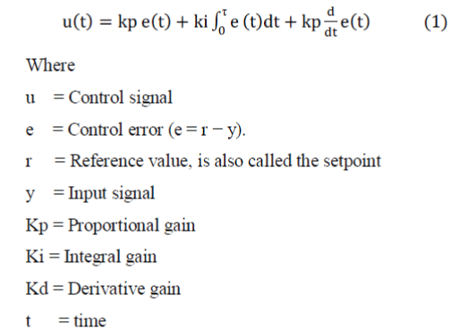 |
| In order to simplify the circuit analysis of the proposed converter with boosting stages, the following
assumptions are made. |
| (1) The coupled inductor T1 & T2 are represented as a magnetizing inductor Lm & Lm1. |
| (2) Lk1 & Lk2 are Primary & Secondary Leakage Inductors of coupled inductor T1. |
| (3) Lk3 & Lk4 are Primary & Secondary Leakage Inductors of coupled inductor T2. |
| (4)All components are ideal, except for the leakage inductance of coupled inductors T1, T2 which is being taken under
consideration. The on-state resistance RDS(ON) and all parasitic capacitances of the main switch S1 are neglected, as are
the forward voltage drops of diodes D1 ∼ D5 . |
| (5) The capacitors C1 ∼ C5 are sufficiently large that the voltages across them are considered to be constant. |
| (6) The ESR of capacitors C1 ∼C5 and the parasitic resistance of coupled inductors T1, T2 are neglected. |
OPERATING PRINCIPLES OF THE PROPOSED CONVERTER |
| In this section the five operating modes of the proposed converter are explained in brief .The operating
principle of continuous conduction mode (CCM) is presented in detail.. There are five operating modes in a switching
period. The operating modes are described as follows. |
| MODE – I (T0 – T1) |
| Fig 2(a) shows proposed converter operating in mode 1.In this transition interval, When S1 & S2 are at ON
state the magnetizing inductor Lm & Lm1 continuously charges capacitor C2 & C4 through T1 & T2.The source
voltage Vin crosses the magnetizing inductor Lm , Lm1 and primary leakage inductor Lk1 ,Lk3.The magnetizing
inductor Lm & Lm1 transfers its energy through coupled inductor T1 & T2 to charge switched capacitor C2 & C4.As a
result the current ILm & ILm1 is decreases |
| MODE – II (T1 – T2) |
| Fig 2(b) shows proposed converter operating in mode 2 .During this transition interval the source voltage
Vin crosses the magnetizing inductor Lm ,Lm1,primary leakage inductor Lk1 ,Lk3 and Primary windings N1
& N3 and acts series with secondary winding N2 & N4 of coupled inductor T1 & T2, Capacitor C1, C2, C3 &
C4. Magnetizing inductor Lm & Lm1 is also receiving energy from Vin. The energy is finally discharged to Output
Capacitor C5 and Load R.As a result the current ILm & ILm1, Ilk1 & Ilk3, Rectifier Diode Current Id5 are increasing.
This mode ends when switch S1 & S2 are turned OFF. |
| MODE – III (T2 – T3) |
| Fig 2(c) shows proposed converter operating in mode 3 .During this transition interval the switches S1 & S2
are in OFF state ,Energy of secondary leakage inductor Lk2 & Lk4 is series connected with C2 & C4 to
charge output capacitor C5 and the load R. Energy stored in Primary leakage inductor Lk1 & Lk3 flows
through diode D1 & D3 to charge capacitor C1 & C3. Ilm and Ilm1 are increasing because magnetizing inductor Lm
and Lm1 is receiving energy from Lk1 & Lk3.Diode D1 and D3 are conducting. This Mode ends when Leakage
Current ILk2 & ILK4 decreases to zero. |
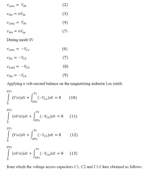
| MODE – IV (T3 – T4) |
| Fig 2(d) shows proposed converter operating in mode 4 .During this transition interval the leakage energy
from the Leakage inductor Lk1 & Lk2 flows through the diodes D1 & D3 keeps charging capacitor C1 & C3 as a result
Currents ILk1, ILK3 and ID1, ID3 are continually decreasing. The Lm & Lm1 is delivering its energy through T1, T2
and D2, D4 to charge capacitor C2 & C4.Diodes D1, D2, D3 & D4 are conducting. The energy stored in output capacitor C5 is constantly discharged to the load R.These energy transfers result in decrease of ILk1, ILK3 and ILm,
ILm1 but increases in ILk2 & ILk4 .This mode ends when current ILk1 and ILK3 reaches zero. |
| MODE – V (T4 – T5) |
| Fig 2(e) shows proposed converter operating in mode 5 .During this transition interval Magnetizing inductor
Lm & Lm1 are constantly releasing its energy to C2 & C4.Diode D2 is conducting. The magnetizing inductor energy
flows through the secondary winding of the coupled inductor N2, N4 and D2, D4 continues to charge capacitor C2. As
a result the iLm & iLm1 are decreasing. The energy stored in capacitor C3 is constantly discharged to the load R.This
mode ends when switch S1 is turned ON. |
STEADY-STATEANALYSIS OF PROPOSEDCONVERTERS |
| To simplify the steady-state analysis, only modes II and IV are considered for CCM operation, and the leakage
inductances on the secondary and primary sides are neglected. The following equations can be written from Fig. 3(b): |
 |
 |
| Both [10] and [11] are employing coupled inductor topology as the boost type converter integrating with coupled
inductor; this technology is similar to the technology of the proposed converter. |
| During CCM operation, the voltage stresses on S1, S2 and D1∼ D4 are given as |
 |
SIMULATION MODEL OF.PROPOSED CONVERTER |
| The simulink model of proposed converter is shown in Fig. 3.It consists of the windings N1,N3 and N2 ,N4
are primary and secondary windings of a coupled inductor T1 ,T2 is similar to the input inductor of the conventional
boost converter, and LK1 LK2 LK3 LK4 are leakage inductors and Lm1,Lm2 is magnetizing inductance. And the
diodes D1 D2 D3 D4 D5 and capacitor C1 C2 C3 C4 C5 are present. Capacitor C1 C3 and diode D1 D3 receives
leakage inductor energy from N1 N3.The secondary winding N2 N4 of coupled inductor T1 T2 is connected with
another pair of capacitors C2 C4 and diode D2 D4, which are in series with N1 N3 in order to further enlarge the boost
voltage. The rectifier diode D5 connects to its output capacitor C5.The output of the converter is summed with
reference voltage and the resulting error is fed to the pi controller. The output of the PID controller is summed with
triangle pulse and later it is fed as gating pulse for the mosfet switch. The Powergui block is necessary for simulation of
any Simulink model containing SimPowerSystems™ blocks. It is used to store the equivalent Simulink circuit that
represents the state-space equations of the model. Here the powergui used is in continues form. IT also consists of
voltage measurement and current measurement block measures the instantaneous voltage and current between two
electric nodes. The output provides a Simulink® signal that can be used by other Simulink blocks. |
RESULTS |
| The electrical specifications are Vin = 15 V,Vo = 250 V,Fs = 50 kHz, RL = 1000Ω. C1=C2=C3=C4=47μF, C5
=220μF.N = 8, D is derived as 55%,P=0.001,I=0.001 |
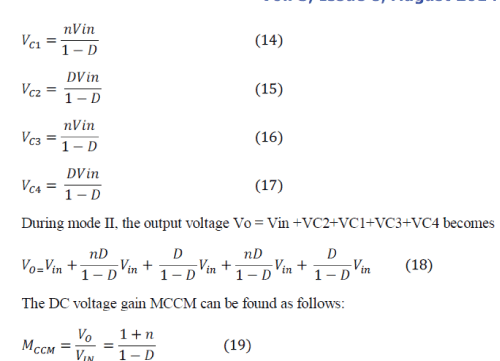
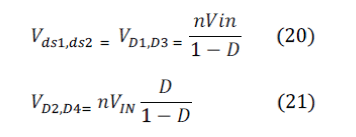
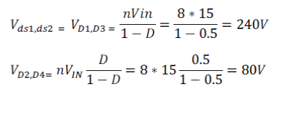
| FIG 4 shows the voltage across diodes D1, D2, D3, D4.The x axis represents time in seconds and y axis
represents voltage in volts. From fig 5 it can observe that voltage across diode D1, D3 is 240v and voltage across diode
D2, D4 is 80v.Voltage across the diodes can be calculated from equations (20) and (21) |
 |
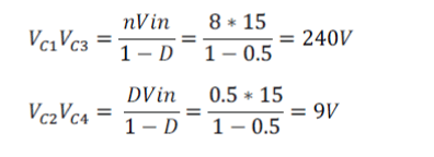
| FIG.5 shows the voltage across capacitors C1, C2, C3, and C4. The x axis represents time in seconds and y
axis represents voltage in volts. From fig 5 it can observed that voltage across capacitors C1, C3 is 240v and voltage
across capacitor C2, C4 is 9v.Voltage across the capacitors can be calculated from equations (14) and (15). |
 |
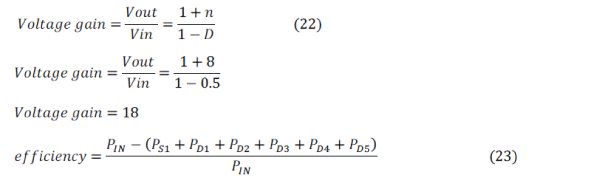
| FIG.7 shows the output voltage of the proposed converter. The x axis represents time in seconds and y axis
represents voltage in volts. From fig 6 it can observe that output voltage of proposed converter is 250V.The voltage
gain and efficiency can be calculated by the equation 22 and 23. |
 |
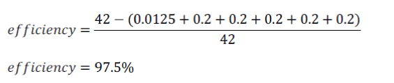 |
| Thus it is observed from equation (22) without extreme duty ratios and the numerous turns-ratios of a coupled
inductor, this converter achieves a high step-up voltage-conversion ratio; the leakage inductor energy of the coupled
inductor is efficiently recycled to the load and they is very low ripple content in the output . |
CONCLUSION |
| This paper has introduced and developed an interleaved high step up dc dc converter with PID controller. The proposed
interleaved high step up DC-DC converter model along with PID controller is modeled using SIMULINK .The
simulation and experimental results show that from the interleaving connection reduction in the input ripple current is
achieved and the energy of the coupled inductor’s leakage inductor has been recycled, the voltage stress selected across
the active switch S1, S2 is constrained, which means low ON-state resistance RDS (ON) can be selected. Thus,
improvements to the efficiency of the proposed converter have been achieved. From the converter, the turns ratio n=8
and the duty ratio D is 55%; thus, without extreme duty ratios and turns ratios, the proposed converter achieves high
step-up voltage gain, and also reduction in the rise time and steady state error is achieved due use of PID controller in
feedback. The experimental results show the efficiency of the converter is 97 %. |
Figures at a glance |
 |
 |
 |
 |
| Figure 1 |
Figure 2 |
Figure 2a |
Figure 3 |
 |
 |
 |
| Figure 4 |
Figure 5 |
Figure 6 |
|
References |
- Shrud, H. Kharaz, A. S. Ashur, A. Faris and M. Benamar, “A study of Modeling and Simulation for Interleaved Buck Converter”, 1st PowerElectronic& Drive Systems & Technologies Conference, Page(s): 28 –35, 2010
- Yabin Zhang, PaolBagnoli, Emilio Franchi.”Theoretical Design of Compact Multi-phase Interleaved Buck DC-DC Converter for AutomotivePower Applications” International Symposium on Power Electronics, Electrical Drives, Automation and Motion (SPEEDAM), 2012, Page(s): 1324 –1329.
- Wennan Guo, Praveen K. Jain, “Analysis and Modeling of Voltage Mode Controlled Phase Current Balancing Technique for Multiphase VoltageRegulator to Power High Frequency Dynamic Load”Applied Power Electronics Conference and Exposition, 2009. APEC 2009. Twenty-FourthAnnual IEEE Pages: 1190 – 1196.
- J.-P. Lee, B.-D. Min, T.-J. Kim, D.-W. Yoo, and J.-Y. Yoo,“Design and control of novel topology for photovoltaic dc/dc converter with highefficiency under wide load ranges,” J. Power Electron., vol. 9, no. 2, pp. 300–307, Mar. 2009.
- O. Hegazy, J. Van Mierlo, P. Lataire, "Analysis, Modeling,and Implementation of a Multidevice Interleaved DC/DC Converter for Fuel CellHybrid Electric Vehicles," IEEE Trans. Power Electron., vol. 27, no. 11, pp. 4445-4458, Nov. 2012.
- Erickson R., Maksimovic D., Fundamentals of Power Electronics. Second Edition, USA: Kluwer Academic Publishers, 2001, pp. 42-45.
- SanjayaManiktala. Switching Power Supplies A to Z M]. Elsevier 2006: 51-54
- X. Kong and A. M. Khambadkone, “Analysis and implementation of a high efficiency, interleaved current-fed full bridge converter for fuel cellsystem,” IEEE Trans. Power Electron., vol. 22, no. 2, pp. 543–550, Mar. 2007.
- Y. T. Chen, S. M. Shiu, R. H. Liang, "Analysis and Design of a Zero-Voltage-Switching and Zero-Current-Switching Interleaved BoostConverter,"IEEE Trans. Power Electron.,vol. 27, no. 1, pp. 161-173, Jan. 2012.
- S. Park, Y. Park, S. Choi, W. Choi, K. B. Lee, "Soft-Switched Interleaved Boost Convertersfor High Step-Up and High-PowerApplications,"IEEE Trans. Power Electron., vol. 26, no. 10, pp. 2906-2914, Oct. 2011.
- P. W. Lee, Y. S. Lee, D. K. Cheng,and X. C. Liu, “Steady-state analysis of an interleaved boost converter with coupled inductors,” IEEE Trans.Ind. Electron., vol. 47, no. 4, pp. 787–795, Aug. 2000.
- D. K. W. Cheng, X. Cu, and Y. S. Lee, “A new modifiedboost converter with ripple free input current by using coupled inductors,” in Proc.IEEE Int. Conf. Power Electron. Variable Speed Drives, London, U.K., Sep. 1998, pp. 592–599.
- F. Yang, X. Ruan, Y. Yang, Z. Ye, “Interleaved Critical Current Mode Boost PFC Converter with Coupled Inductor,” IEEE Trans. PowerElectron., vol. 26,no. 9, pp. 2404–2413, Sep. 2011.
|