Keywords
|
| Microstrip patch, array antenna, IE3D, WiMAX, FR-4 Substrate. |
I.INTRODUCTION
|
| Parallel to the rising importance of wireless communication systems and personnel IT (information technologies) services (e.g., Bluetooth) increasing efforts are devoted to the design and implementation of novel Microstrip structures from miniaturized electronic circuits to the antenna arrays. One major application is design of Microstrip antenna arrays which are attractive candidates for adaptive systems in the present and future communication systems. Their main advantages are light weight, low cost, planar or conformal layout, and ability of integration with electronic or signal processing circuitry [1]. This design of Microstrip array antenna is for WiMAX and WLAN applications. The Microstrip patch antenna is design at resonant frequency of 3 GHz, This designed added mutual coupling into account of simulated results. The Microstrip patch antenna offers a low profile, i.e. thin and easy manufacturability, which provides a great advantage over traditional antennas. |
| Patch antennas are planar antennas used in wireless links and other microwave applications [1]-[3]. The low profile feature of the patch antenna leads to a relatively narrow bandwidth. In addition, the performance of such design can be improved by selecting proper geometry of the patch [2]. The design and estimation of the parameters of a Microstrip patch antenna is generally complex and requires detailed mathematical approach for full-wave analysis. The antenna dimensions are critical in the quantitative estimation of the desired antenna performance with the desired accuracy in results. |
| Microstrip arrays are limited in that they tend to radiate efficiently only over a narrow band of frequencies and they cannot operate at the high power levels of waveguide, coaxial line, or even strip line [4]. In various communications and radar systems Microstrip antenna is greatly desired. Microstrip antennas are very versatile and are used, among other things, to synthesize a required pattern that cannot be achieved with a single element. In addition, they are used to scan the beam of an antenna system, increase the directivity, and perform various other functions which would be difficult with any one single element. The elements can be fed by a single line or by multiple lines in a feed network arrangement. The first is referred to as a series-feed network while the second is referred to as a corporate-feed network. |
| A standard approach to design arrays consists in the design of the array element and a feeding network [ l ] .The main weakness of an ordinary Microstrip element is its narrow bandwidth. There are several ways of how to overcome this problem. A well-known way is based on the introduction of an additional stacked or coupled patch. This makes the configuration more complex. As a consequence the array becomes more costly in production especially in the case of stacked patches. Also the dimension of the may increases. An alternative way consists in the use of specially shaped patches. There are two different types of patches: specially shaped patches with slits (for example E-shaped patches) and rectangular patches with slots. We have considered the E-shaped patches because they have a wider bandwidth and they are simpler in production. In order to keep the size of the array small, we have chosen a special combined series /corporate feed network where all patches are linked in series and the coaxial feed is connected to the second patch. |
II. LITEARTURE REVIEW
|
| Deschamps first proposed the concept of the MSA in 1953.A patent was issued in France in 1955 in the names of Gutton and Baissinot [1]. Shortly thereafter, Lewin investigated radiation from strip line discontinuities. Additional studies were undertaken in the late 1960âÃâ¬ÃŸs by Kaloi, who studied basic rectangular and square configurations and other than the original Deschamps report, work was not reported in the literature until the early 1970âÃâ¬ÃŸs, when a conducting strip radiator separated from a ground plane by a dielectric substrate was described by Byron. However, the first practical antennas were developed by Munson and Howell in the 1970s [1]-[2]. Weinschel developed several Microstrip geometries for use with cylindrical S band arrays on rockets. Sanford showed that the Microstrip element could be used in conformal array designs for L band communication from KC-135aircraft to the ATS-6 satellite. Additional work on basic Microstrip patch elements was reported in1975 by Garvin et al, Howell, Weinschel and James and Wilson. The early work by Munson on the development of Microstrip antennas for use as low profile flush mounted antennas on rockets and missiles showed that this was a practical concept for use in many antenna system problems. |
| In recent years the design of Microstrip patch array antenna has attracted many researchers in the field of Wireless communication. In a previous work, Shen and Vandenbosch have used the electric field distribution on top surface above a superstrate to determine its shape and size that minimize its edge diffraction. MSAs have narrow BW, typically 1–5%, which is the major limiting factor for the widespread application of these antennas. Increasing the BW of MSAs has been the major thrust of research in this field, and broad BW up to 70% has been achieved [2]. |
III.DESIGN METHODOLOGY
|
| The designed antenna is 2 element E shaped Microstrip patch antenna array. The first step in the design is to specify the dimensions of a single Microstrip patch antenna. The patch conductor can be assumed at any shape, but generally simple geometries are used, and this simplifies the analysis and performance prediction. Here, the half-wavelength rectangular patch element is chosen as the array element (as commonly used in Microstrip antennas) [4]. Its characteristic parameters are the length L, the width w, and the thickness h. |
| To meet the initial design requirements (operating frequency = 2.4 GHz, and beam width = 90) various analytical approximate approaches may be used. Here, the calculations are based on the transmission line model [9]. Although not critical, the width w of the radiating edge is specified first. In practice, the length L is slightly less than a half wavelength (in the dielectric). The length may also be specified by calculating the half wavelength value and then subtracting a small length to take into account the fringing fields. |
| Therefore many kinds of miniaturization techniques, such as using of high dielectric substrates, resistive or reactive load and increasing the electrical length of the antenna, also it gives a good directivity and high gain with good performance characteristics [5].The proposed array Antenna will be working on 2.45 GHz frequency range. i.e.(ISMband) and The patch resonance to produce a broadband response. Representative results for the VSWR response, Sparameter and radiation patterns are shown in Figures 2, 3 and 4. The gain of the antenna is higher than the traditional Microstrip antenna [6]. |
| Theoretical analysis and calculation of a single Microstrip patch is calculated with following equations [7]: The first step is to find the width, W of the patch at the resonant frequency using Equation 1: |
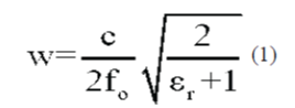 |
| Where, εr is the relative permittivity of the substrate, c is the speed of the light in free space and fo is the resonant frequency, Length of the patch is calculated by Equation 2; |
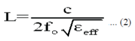 |
| Where, εeff is the effective dielectric constant of the substrate. To measure for the fringing effects, the actual length of the patch also includes the correction factor due to fringing effect. Actual length is given by Equation 3; |
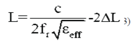 |
| Correction factor can be found using the equation 4; |
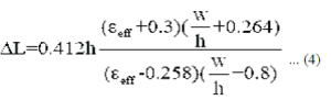 |
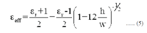
| Where, h is the height of the substrate and εeff is effective dielectric constant used in equation 4 is given by Equation 5; |
 |
| Ground patch of the geometry is design with the following equation 6; Length and width of ground patch, |
| Lg = 6h+L .....(6.a) |
| Wg = 6h+W ...... (6.b) |
| The dimensions for designing a single Microstrip patch are tabled below: |
| Figure 2 show the geometry of inset feed Microstrip array antenna with two patches in the array. The patch is energized electromagnetically using 50 ohm SMA connector. Hence wide bandwidth is generated as the resonant circuits become coupled [8]. The slots aggregate the currents, which give additional inductance controlled by the patch width. IE3D software has been used to calculate the return loss (S 11), directivity vs. frequency, 3D radiation pattern & field gain Vs frequency [9]. |
| The present work signifies that by introduction of two Patch in the same size [10], the Directivity gets enhanced about 9bdB i.e., Figure 3 shows the return loss (S11) vs. frequency curve for the proposed inset feed Microstrip patch antenna The positions of the slots were varied to see the effect on the Microstrip antenna bandwidth. It was observed that antenna performance could be controlled by introducing slots to a large extent in terms of increased bandwidth, As the slots move in Y direction the bandwidth gets increases for the proposed design [11]. From the present work it can b e inferred that as the slots are moving along the Y axis in both the directions, of course in specified range the bandwidth and other performance parameters are also improving significantly. |
III.SIMULATION RESULT
|
| The proposed geometry of Microstrip phased array antenna designed with IE3D and simulation is performed [12]. At the resonant frequency of 3 GHz the design is simulated in the frequency range of 1 to3 GHz. |
| In the fig 3, it shows the graph of simulated return loss Vs frequency for the proposed Microstrip patch array. Reflection coefficient (S11) or return loss is defined as the ratio of reflected power to the incident power. The Simulated return losses of proposed array is -24.074 dB at 2.36391 GHz. This low value of return loss yields higher efficiency in WLAN applications [13]. |
| In the fig 4, it shows the graph of VSWR Vs frequency. VSWR is obtained near about 1. The Voltage Standing Wave Ratio (VSWR) is an indication of the amount of mismatch between an antenna and the feed line connecting to it. The range of values for VSWR is from 1 to ∞. A VSWR value under 2 is considered suitable for most antenna and wireless |
| applications. The antenna can be described as having a good match. VSWR is exactly obtained 1.14656 at 2.36391 GHz (less than 2). |
| In the fig.5, the graph shows the Impedance matching in Smith chart. The Smith Chart is a sophisticated graphic tool for solving transmission line problems. One of the simpler applications is to determine the feed-point impedance of an antenna, based on an impedance measurement at the input of a random length of transmission line [14]. By using the Smith Chart, the impedance measurement can be made with the antenna in place atop a tower or mast, and there is no need to cut the line to an exact multiple of half wavelengths. |
| In fig.6, it shows the graph of Y – Parameter Vs frequency. Y – Parameter or Admittance Parameter of proposed array is obtained 0.020 Simens. |
| In fig.7, it shows the graph of Z – Parameter Vs frequency. Z – Parameter or Impedance Parameter of proposed array is obtained 50 ohm [15]. Simulated and measured results satisfy the requirements of wireless communication. |
VI.CONCLUSION
|
| This design can be implement for LTE (4G), WiMAX and WLAN application with mutual coupling [16]. Consequently the feeding network can be greatly simplified. A good design of the antenna can improve overall system performance. Many factors must be considered such as operating frequencies, bandwidth requirements of the antenna system, and directivity, all of which affect its efficiency. In this paper an integrated 2.4 GHz phased array antenna with multiple layers are proposed for a wireless system. |
VII.ACKNOWLEDGEMENT
|
| The authors would like to give million thanks for Mrs. Sweta Agarwal Ali as project supervisor for his contribution, guidance, support, commitment, constructive support and encouragement upon accomplishment of this project. Millions thanks also to everyone for their helps and supports in completing this project especially to Electronics & Communication Department of Invertis University, Bareilly. |
| |
Tables at a glance
|
 |
| Table 1 |
|
| |
Figures at a glance
|
 |
 |
 |
 |
| Figure 1 |
Figure 2 |
Figure 3 |
Figure 4 |
 |
 |
 |
| Figure 5 |
Figure 6 |
Figure 7 |
|
| |
References
|
- RameshGarg, PrakashBhartia, InderBahl, “Microstrip Antenna Design Handbook,” Artech House Publication.
- Girish Kumar, K. P. Ray, “Broadband Microstrip Antennas,” 2003 Artech House, Inc.
- Balanis “Antenna Theory - Analysis and Design,” 2006.
- L. Stark, “Microwave Theory of Phased-Array Antennas- A Review,” Proc. IEEE, vol. 62, pp. 1661–1701, December 1974.
- ZhongkunMa , Vladimir Volski, Guy A. E. Vandenbosch, “Optimized Design of a Compact Low-cost 4 Element Microstrip Antenna Arrayfor WLAN,” 2010 URSI International Symposium on Electromagnetic Theory, pp.573-576.
- N.fishahAbWahab, ZulkifliMaslan, W. Norsyafizan W. Muhamad, NorhayatiHamzah, "Microstrip Rectangular 4x1 Patch Array Antenna at2.5GHz for WiMax Application,” 2010 Second International Conference on Computational Intelligence, Communication Systems andNetworks.
- F. M. Kashif, W. Qadeer, and S. I. Shah, “Efficient implementation of quadrature amplitude modulation transmitters,” IEEE INMICTechnology for the 21st Century, 2001.
- W. Aerts, P. Delmotte, G. A. E. Vandenbosch , “Conceptual Study of Analog Baseband Beam Forming: Design and Measurement of an Eightby-Eight Phased Array,” Transaction on Antenna Propagation, vol. 57, No. 5, pp. 000-999, 2009.
- Aliakbarian, V. Volski, E. van der Westhuizen , R. Wolhuter, and G. A. E. Vandenbosch , “Analogue versus Digital for Baseband BeamSteerable Array used for LEO Satellite Applications”.
- POZAR D.M., and SCHAUBERT D.H., “Microstrip Antennas, the Analysis and Design of Microstrip Antennas and Arrays,” IEEE Press,New York, USA, 1995.
- Guru Parsad, Tirupathi. “Design, Analysis and Study of 2x2 Rectangular Microstrip Antenna Array At 430 MHz for Wind Profiler RADAR,”International Journal of Computer Applications & Information Technology Vol. 1, No.1, July 2012.
- J.R.JAMES, P.S.HALL and C.WOOD, “Microstrip Antenna Theory and Design,” London, UK: Peter Peregrinus, 1981.
- M. Amman, “Design of Microstrip Patch Antenna for the 2.4 GHz Band, Applied Microwave and Wireless,” pp. 24-34, November /December1997.
- JAMES J.R., and HALL P.S., “Handbook of Microstrip Antennas,” Peter Peregrinus Ltd., London, UK, 1989.
- Mailloux, R. J., J. F. Mcllvenna, and N. P. Kernweis, “Microstrip array technology," IEEE Antenna Propag., Vol. 29, No. 1, 25{27, January1981}.
- Slomian, I. Piekarz, K. Wincza, and S. Gruszczynski, “Microstrip antenna array with series feeding network designed with the use ofslotcoupled three-way power divider,” IEEE Antennas Wireless Propag. Lett., vol. 11, pp. 667–670, 2012.
|