INTRODUCTION
|
| There is a demand for product authentication, security, and reliability of the electronic system. In 2012, IHS isupply ranked counterfeited electronic devices as, analog ICs (25.2%), microprocessors (13.4%), memory ICs (13.1%), PLDs (8.3%). Now a days most of the systems like ATM, Smart card, RFID tag using Printed serial numbers for identification. With ever increasing the growth, the counterfeit also get increased due to that the process of using printed serial numbers system for identification in most of the systems. |
| The most of the companies and industries are affected as directly. The person who has more hope from the organization, they do this counterfeiting. That most believable person theft the secrets and confidential data, and sell that to the other company or any organization. Due to that, they can easily copy and clone that product. It may be work on good manner. But the product designers get affected as physically and mentally. To avoidthese counterfeiting problems, here the PUF (Physical Unclonable Function) system introduced. |
| The main objective of this paper is to produce more secured system at low cost authentication and device must not be copied and cloned. The products are secured highly but in cheapest way and can be used for high level security. Goal is avoid the counterfeiting occur in an electronic device.PUF technology provides a secure method for storing a key withstanding today attacks and even protecting against future potential attacks. |
| PUF is defined as a function based on physical characteristics. It is unique for each chip, difficult to predict, easy to evaluate, easy to make, and reliable. It is practically impossible to duplicate. This is used for secure chip authentication. It is one-way function. It has unique and unpredictable way of mapping challenges and response. PUF has more environmental variations like temperature variation, power supply voltage, Electromagnetic interference. PUF can serve a root of trust and provide a key which cannot be easily reverse engineered. It is used for prominent and secure applications. |
| The organization of this paper is as follows. In section II we discuss about the previous studies related to our subject and discussion. In section III we describe about the proposed work and the device descriptions which are present in the block diagram and finally we show the result analysis in section IV. |
RELATED WORKS
|
| The most dominant approaches for implementing PUF either leverage the bi-stable circuit element such as SRAM arrays [1, 2], or are based on variations in logic gate / wire delays or leakage currents [3, 4]. The PUF in [3] utilized delay difference between pairs of parallel timing paths with equal nominal delay. PUF bits were generated by a delay arbiter connected to these paths. To increase the number of CRPs, the paths were segmented and multiplexed by challenge bits. An ASIC implementation was demonstrated in 180nm CMOS [7]. The US government and semiconductor companies point out potential system susceptible to danger resulting from the contract foundry model, hardware intellectual property and IC theft, as well as counterfeiting [5, 6]. Further aspects of PUF design, performance and security foundations applicable to our work can be found in [8, 9, 10]. |
PROPOSED SYSTEM
|
| In this section we have to discuss about our work related to this paper. Full details are explained in the overview of the PUF |
| A. BLOCK DIAGRAM |
B. OVERVIEW
|
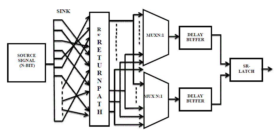
| Here we introduce our proposed PUF architecture. For introducing PUF we need clock network. A clock PUF compares the arrival time of the clock signal and generates the stable but unclonable bits. A figure shows the flow of the clock PUF. The major components of our paper are explained below. |
| • The source signal is given to the clock network. Source signal is in the form of binary digits. That signal is branched out and inserted to the sink without affecting the clock network. |
| • The return path catches the signal from the sink and passes it to the mux network. The return path has even number of inverters. Here return paths are buffered and accumulate the process variation from different region of the chip. |
| • The multiplexer network is selecting two clock signal and compare it. The clock signal is distributed with the pair of adjacent multiplexors or using distributed multiplexors. |
| • A pair of externally controlled delay buffers with matched delays to maximize the variation. |
| • The result from the buffer is given to the SR-latch to determine which of two signal transitions first. |
| In this clock PUF the sink is selected then connected to the return path as carefully, to get equal propagation delay and matched length. There is not necessary to connect the sink result as directly to the return path we can connect the result of the sink to any node of return path for increasing the security level. The mux arbiter compares pairs of clock transition and producing a bit at a time. It pass through the delay buffer which can compensate for unintentional systematic delay encountered on the way. At the end of the architecture a latch is connected. |
C. DEVICE DESCRIPTIONS
|
| The following devices are present in the clock PUF architecture. They are explained detail manner in following sessions. The devices are |
| • Source of clock network (input) |
| • Sinks |
| • AND gate |
| • Multiplexer |
| • Tunable Delay buffer |
| • SR Latch |
| • Source of Clock Network: Source is the input of the clock network. An input is given like a binary bit. It can be split in number of levels depends on input. This process will continue up to get single bit separation. This separated bit is given to the input of sink. Sink has flip-flop & AND gate combination network. |
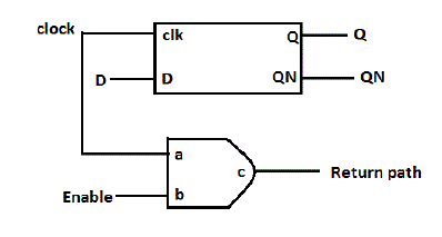
| • Sink: It is the combination of flip-flop & AND gate network. Each bit which is split from the clock source given to the input of the sink. Number of sink network used here depends on the clock source. Because each split bits require a sink network. The output of the sink network is given to the input of the return path. Sink network is given in fig.2. |
| • Return Path: Return path of the clock PUF architecture is used to pass the input value to the output as without change in input value. But can connect any output of the sink to any input of the return path. Due to that the data changes and correction can be conducted by designer only, others don’t get idea about the internal connection. So security can be increased depends on the connection. |
| In return path network, even number of inverters are connected depends on the designer. By connecting the inverters as even manner, can get the output as same as the input otherwise the response get varied. The output of the return path is given to the input of the multiplexer |
| • Multiplexer: The term multiplexer means many to one. Multiplexing is the process of transmitting a large number of information over a single line. A digital multiplexer (MUX) is combinational circuits that select digital information from several sources and transmits the selected information on a output line. A multiplexer is also known as a data selector since it selects one of many inputs and steers the information to the output. |
| The multiplexer has several data input lines and single output line. The selection of a input line is controlled by a set of selection lines. The selection line decides the number of input lines of a particular multiplexer. If the number of n input lines is equal to 2m, then m select lines are required to select one of the n input lines. |
| • Delay Buffer: Delay buffer act as a buffer with some delay. It has single input and single output signal. But it gives the output signal with some delay. |
| • SR Latch: In this paper we use SR-Latch. SR latch have two inputs, S and R. S and R is called set and reset respectively. The S input is support to produce HIGH on Q (i.e. store binary 1 in flip-flop). The R input is support to produce LOW on Q (i.e. store binary 0 in flip-flop). Q' is complementary output of Q, so it always holds the opposite value of Q. The output of the S-R latch depends on current as well as previous inputs or state, and its state (value stored) can change as soon as its inputs change. |
D. IMPLEMENTATION
|
| By using the above unclonable bit we can generate cryptography key. This unclonable bit can control the devices which need more security. The generated unclonable bit given to the input of external devices, it controls that device as internally. If anyone wants to copy that secured device means they cannot copied as correctly due to that internal variation and cannot be cloned too. Thus that device gets most security and can be withstanding in their unique character. |
SIMULASION RESULT
|
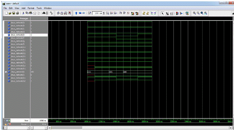
| For simulate this paper we use ModelSim. From the block diagram we know that each level needs the result of the previous level to respond to the next level. The source signal has n-bit binary value as input. It split into a single bit then passes it to the return path through the sink. Then send it to the mux network for getting result as unclonable bit. |
| A pair of delay buffers at the inputs of the delay arbiter compensates for the intrinsic delay difference between paths. When nominal delays of two return paths are matched, their comparison generates a random bit. Small biases in such bits can be tolerated by combining multiple bits. The best settings of delay buffers are determined empirically based on a sufficiently large lot of chips. By setting delays to median values, one decreases systematic bias in delay differences and increase variation entropy available for PUF bit generation. To further increase entropy, several settings for delay buffers can be used. Using such settings as a challenge response mechanism repeals attacks based on replaying or analyzing responses to a single setting. Finding good settings of delay buffers and PUF read-out does not require external tools when delay buffers can be programmed via multiplexed input pins. |
CONCLUSION
|
| In this project we introduce PUF system based on clock network for security purpose. This PUF system ensures product authenticity, security and reliability of the electronic system. Now a days, lots and lots of companies are emerging and they produce products (circuit devices) for mobile, laps, iPhone etc., but the original product designer not getting the merit for their product due to a major problem called counterfeiting. To avoid that problem we proposed a PUF system using clock network. This circuit produce security key and protect the device from cloning. If the system attempt to be copied by someone, they can’t get the exact functionality of the system. Hence the product with PUF cannot be cloned. It is implemented in RFID technology and can be implemented in finger print, smart card system, etc., also. Our government accepts this product for the security purpose. Recently this PUF receive particular attention in the chip market as a promising way to provide security. Hence we implement PUF system to avoid counterfeiting and protect the products in an efficient way. |
Figures at a glance
|
 |
 |
 |
| Figure 1 |
Figure 2 |
Figure 3 |
|
| |
References
|
- J. Guajardo, S.S. Kumar, G. Schrijen, and P. Tuyls. FPGAintrinsic PUFs and their use for IP protection. In CryptoHardware &Emb Sys (CHES), pages 63–80, 2007.
- D.E. Holcomb, W. Burleson, and K. Fu. Power-up SRAM state as an identifying fingerprint and source of truerandom numbers. IEEE Trans. Comp., 58(9):1198–1210, September 2009.
- B. Gassend, D. Clarke, M. van Dijk, and S. Devadas. Controlled physical random functions. In ACSAC, pages149–160, 2002.
- G. Suh and S. Devadas. Physical unclonable functions for device authentication & secret key generation. In DAC, pages 9–14, 2007.
- Defense Science Board (DSB) study on High Performance Microchip Supply, 2005.
- Defense Industrial Base Assessment: Counterfeit Electronics study by U.S. Dept. Of Commerce Bureau OfIndustry & Security Office Of Tech. Evaluation, 2010.
- J.W. Lee, A. Lim, B. Gassend, G.E. Suh, M. van Dijk, and S. Devadas. A technique to build a secret key in integrated circuits for identification and authentication applications. In Symp. VLSI, pages 176–179, 2004.
- R. Maes and I. Verbauwhede. Physically Unclonable Functions: a Study on the State of the Art and FutureResearch Directions. Springer, 2010.
- U. Ruhrmair, S. Devadas, and F. Koushanfar. Security Based on Phys. Unclonability and Disorder. Springer, 2011.
- F. Armknecht, R. Maes, A.-R. Sadeghi, F.-X. Standaert, and C. Wachsmann. A formalization of security features of physical functions. In IEEE Symp.Sec’ty& Privacy, pages 397–412, 2011.
|