Keywords
|
| MOS, Low noise amplifier, Gain, Noise figure, IIP3. |
INTRODUCTION
|
| Low noise amplifier is an electronic amplifier used to amplify possibly weak signals (for example, captured by antennas). It is usually located very close to the detection device to reduce losses in the feed line. LNA plays a key role in overall performance of RF receiver, it is the first component in any RF receiver and it can be implemented using MOS amplifier [6]. |
| Low noise amplifier is designed using 180nm RF MOS technology for ZigBee development. Zigbee is used for high level communication protocols used to create personal area networks built from small, low-power digital radios. ZigBee is based on an IEEE 802.15 standard. ZigBee devices can transmit data over long distances by passing data through intermediate devices to reach more distant, creating a mesh network. ZigBee communication can occur in three bands 868-868.8Mhz or 902-928 MHz or 2.4-2.4834Ghz. This design is mainly concentrated on 2.4 GHz band because global operation occurs in this band. The noise figure of the LNA directly adds to that of receiver. For a typical receiver noise figure of 6 to 8dB, it is expected that the antenna switch or duplexer contributes about 0.5 to 1.5dB, the LNA about 2 to 3dB, and the remainder chain about 2.5 to 3.5dB.while these values provide a good starting point in the receiver design, the exact partitioning of the noise is flexible and depends on the performance of each stage in the chain [6]. LNA is designed to provide a 50 ohms input resistance; this requirement limits the choice of LNA topologies. We cannot begin with an arbitrary configuration, design it for a certain noise figure and gain and then decide to create input matching. |
II.LITERATURE SURVEY
|
| Md.Asif Mahmood Chowdhury et al, designed “A Low Noise Amplifier circuit with high center frequency and ultra wide bandwidth” using IBM 90nm CMOS process during the design the circuit [1]. Centre frequency of this LNA circuit is 18.3GHz. At the Centre frequency Gain is 14.38dB. 5.7 GHz is the -3dB bandwidth of this LNA circuit. It can be operated from around 14.2GHz to around 19.9GHz with considerably high Gain. CS-CS Cascode stage LNA topology is used in the design. Performance of this LNA is verified by HSPICE. Required supply voltage for this LNA circuit is 1.4V. |
| Kai-Wei Ku and Chien-Chang Huang, proposed “A Low power LNA for wireless communications” A low power CMOS LNA working at 2.4GHz for wireless communication is presented in this design, by using TSMC 180nm technology [2]. The current reused architecture is adapted to reduce the consumed current, while the supply voltage is set to 0.6V to meet the low voltage requirement as well. To simplify the bias network designs under low-voltage operations, NMOS and PMOS devices are utilized with three-stage configuration to enhance the Gain performance. The Gain achieved in this design was 17.7dB with a Noise figure of 3.9dB and IIP3 of -17dBm. |
| M.E.Kaamouchi, M.S.Moussa, proposed “A 2.4GHz fully integrated ESD-protected LNA in 130nm CMOS technology”. This paper reviews and analyzes a fully integrated electrostatic discharge (ESD)-protected LNA for lowpower and narrowband applications using a Cascode Inductive source degeneration topology, designed and fabricated in 130-nm CMOS silicon-on-insulator technology [4]. The designed LNA shows 13dB power gain at 2.4 GHz with a noise figure of 3.6 dB and input return loss of -13 dB for power consumption of 6.5mW. |
| A. V. Do, C. C. Boon et al, proposed “A sub threshold LNA optimized for Ultra low power applications in ISM band”. The IEEE 802.15.4 standard relaxes the requirements on the receiver front-end making sub threshold operation a viable solution. The specification is discussed and guidelines are presented for a small area ultra-low-power design. A sub threshold biased LNA has been designed and fabricated for the 2.4-GHz IEEE 802.15.4 standard using a standard lowcost 180nm RF CMOS process [5]. The single-stage LNA saves on chip area by using only one inductor. This design achieves a Gain of 21.4dB with a Noise figure of 5.2dB and IIP3 of -11dBm. |
III. REQUIREMENTS OF LNA
|
| The LNA should provide sufficient gain to minimize the noise contribution from the other blocks following it. The gain should not be too high, because the amplifiers stability due to the unavoidable parasitic feedback loops. The other reason being the high linearity requirements imposed on the succeeding blocks, specifically the down-conversion mixer. LNA should provide proper termination to match the antenna impedance to ensure maximum power transfer and to avoid reflections at the antenna-LNA interface [7]. The LNA should be sufficiently linear so that the intermodulation products generated in the presence of large interface do not degrade the desired weak signal. The LNA should provide sufficient reverse isolation to reduce the local oscillator leakage from the mixer to the antenna, because the leaked local oscillator signal gets reflected by moving objects, gets received by the antenna, mixes with the local oscillator in the mixer and creates time varying DC offset at the mixer output. For Zigbee applications operating at 2.4 GHz LNA should provide a gain better than 15dB and a noise figure of 5dB and IIP3 of -10dBm or -9dBm [5]. |
A. GAIN OF AN AMPLIFIER
|
| Gain is the ability of an amplifier to increase the power or amplitude of a signal from input to output by adding energy to the signal converted from some power supply. It is usually defined as the mean ratio of the signal output of a system to the signal input of the same system. It is often expressed using the logarithmic decibel (dB) units ("dB gain"). A gain greater than one (zero dB), that is, amplification, is the defining property of an amplifier. The voltage gain of an amplifier is expressed as: 20 log (Vout/Vin) dB. |
B. NOISE FIGURE
|
| Noise figure (NF) and noise factor are measures of degradation of the signal-to-noise ratio (SNR), caused by amplifier in a radio frequency (RF) signal chain. It is a number by which the performance of an amplifier can be specified. The noise factor is thus the ratio of actual output noise to that which would remain if the device itself did not introduce noise, or the ratio of input SNR to output SNR.The noise factor F of a system is defined as: F= (SNRin/SNRout), where SNRin and SNRout are the input and output signal-to-noise ratios, respectively. The SNR quantities are power ratios. |
| The noise figure NF is defined as: NF= 10log (F). |
C. IIPn (INPUT REFERRED NTH ORDER INTERCEPT POINT)
|
| Intermodulation is the amplitude modulation of signal containing two or more different frequencies in a system with non-linearities. Intermodulation distortion is characterized by the ratio of the component due to nth order intermodulation to the fundamental component. Another measure related to intermodulation is the Input referred nth order intercept point (IIPn). IIPn are indicators of good linearity in an electronic device like LNA, RF mixers or power amplifiers. Integrated function such as LNA can be built with highest linearity. The design aim is to obtain highest IIP without sacrificing current consumption, gain, and size. Practically speaking describing IIPn order up to 5 can be significant. Today, however the order 3 dominates when describing the normal operation of sensitive devices. |
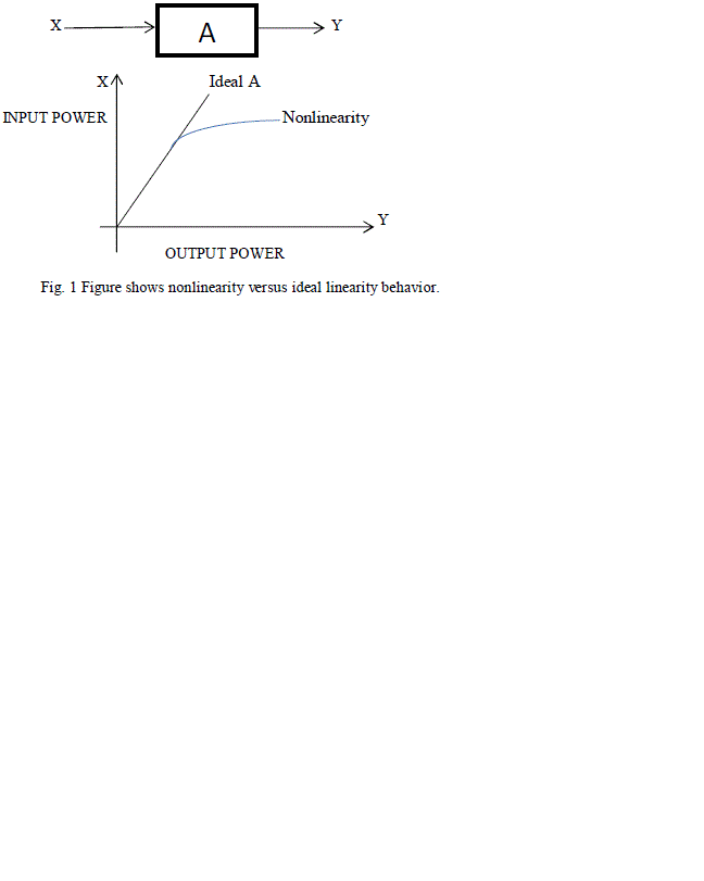
| A Nonlinear amplifier is usually modeled with a power series given by: |
 |
| For a pure linear function Ai=0 for all i >1. I.e. Y(linear) = A0+ A1X. Unfortunately this is never entirely so, the terms X2, X3, X4 etc. are present as well. This magnitudes depends on the strength of A2, A3, A4 etc. and they are responsible for the deviation of the transfer function ‘A’ away from the desired, perfect, proportional law. |
| Assuming x(t) is a sine wave signal x(t) = A cos(ω.t + Φ), by expressing x(t) in its Euler form the second order harmonics ωa+ωb, ωa-ωb can be easily removed by a low pass filter, but it will not be easy (even impossible) to remove the (IM3) 2ωa-ωb and 2ωb-ωa terms because they are embedded in the useful band. This is precisely why in RF the third-order terms are so critical and must be known, measured, and minimized everywhere in the signal chain. |
IV. LNA ARCHITECTURE SELECTION
|
| Noise figure, Input intercept point and Gain constitute the principle targets in LNA design [6]. |
| LNA topologies: |
| 1. Common Source stage with Inductive load. |
| 2. Cascode Stage LNA with Inductive load. |
A.COMMON SOURCE STAGE WITH INDUCTIVE LOAD
|
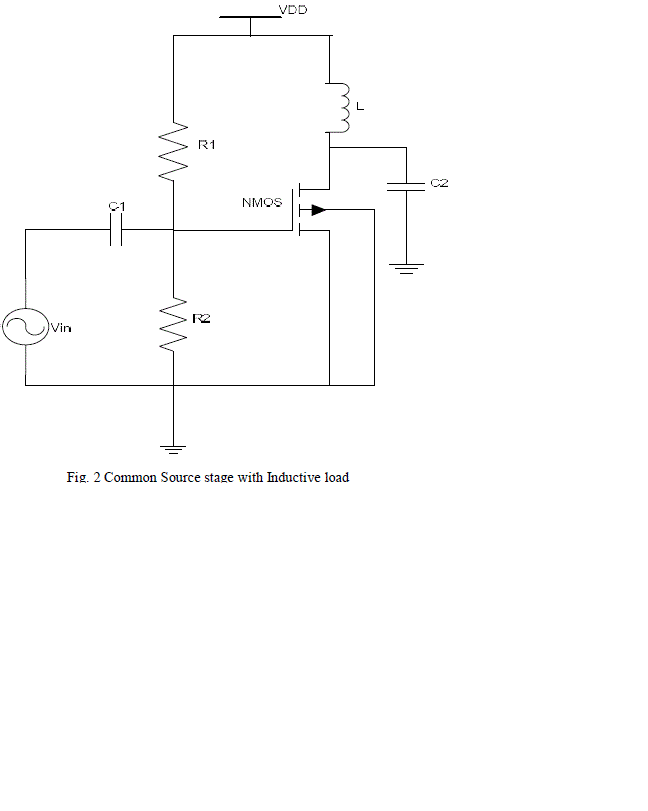
| The common-source (CS) amplifier may be viewed as a trans-conductance amplifier or as a voltage amplifier. As a trans-conductance amplifier, the input voltage is seen as modulating the current going to the load. As a voltage amplifier, input voltage modulates the amount of current flowing through the MOSFET. |
| In Common Source with Inductive load we can tune the LNA to a particular frequency by varying the load Inductance L. By keeping L at 7nH and C2 at 0.6pF circuit is tuned at a frequency of 2.427GHz practically, which is very much suitable for ZigBee applications. |
| DESIGN VALUES: VDD = 1.5V, R1= 100 KHz, R2=50 KHz, L=7nH, C1=0.1uF, C2=0.6pF, W/L=17. |
| Theoretically tuned frequency: ïÿýïÿý = 1/2ïÿýïÿý√ïÿýïÿýïÿýïÿý = 2.455GHz. |
B. CASCODE STAGE LNA WITH INDUCTIVE LOAD
|
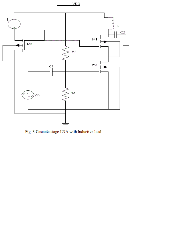
| Cascode stage LNA is constructed using two MOSFET’s, one operating as CS and other operating as CG. Basic idea in this circuit is to combine the high input resistance and large Trans-conductance achieved in a CS amplifier and the superior high frequency response of the CG amplifier. Cascode stage LNA can be used to design a wider Bandwidth, very large output impedance and large voltage swing but equal DC gain as compared to CS amplifier with inductive load. The main advantage of using this circuit is it does not need an external bias, in this LNA a current mirror is used for biasing the MOSFET M1. A current mirror is basically a current amplifier. The reference side of the mirror generates the bias voltages for both the MOSFETs of the Cascode output side. |
| DESIGN VALUES: VDD = 1.3V, R1= 50kHz, R2=50kHz, L=8.4nH, C1=0.1uF, C2=0.5pF, I=1mA, (W/L)1=33, (W/L)2 =16, (W/L)3 =22. |
| In this design by keeping L at 8.4nH and C2 at 0.5pF circuit is tuned at a frequency of 2.449GHz practically, which is very much suitable for ZigBee applications. Theoretically tuned frequency: ïÿýïÿý = 1/2ïÿýïÿý√ïÿýïÿýïÿýïÿý = 2.455GHz. |
V. SIMULATION RESULTS
|
| Simulations are done using HSPICE for both the design with varying inductance value and a plot of frequency versus Gain is observed, Noise figure and IIP3 are calculated for both the designs. |
| A. Frequency versus Gain plot of Inductively loaded CS LNA tuned at 2.427GHz. |
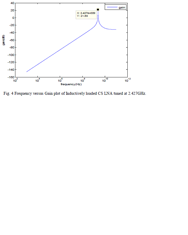
| Frequency versus Gain plot of Inductively loaded Common source LNA tuned at 2.427GHz shown in Fig. 4. This design achieves a Gain of 21.89dB, with an IIP3 of -14.63dBm and Noise factor of 1dB. The most important thing in this design is the LNA is tuned in the ZigBee operation band. |
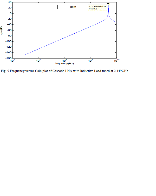
| B. Frequency versus Gain plot of Cascode LNA with Inductive Load tuned at 2.449GHz. |
| Frequency versus Gain plot of Cascode LNA with Inductive Load tuned at 2.449GHz is shown in Fig. 5.This design achieves a higher Gain than the Common Source with Inductive load LNA. Simulation results shows that the circuit achieves a Gain of 34.6dB, with an IIP3 of -10.6dBm, and a Noise factor of 4.3dB. |
VI. CONCLUSION
|
| This paper presents design of LNA working at 2.449GHz by using MOS 180nm PTM technology at level 49. The Cascode with current mirror architecture is adapted in order to reduce the bias voltages required to bias the MOSFETs and to achieve larger Band-width and DC Gain while leaving Gain-bandwidth product unchanged as compared to CS stage. The Cascode stage LNA with Inductive load at 2.449GHz exhibits a large Gain of about 34.6dB with a Noise figure of 4.3dB and an IIP3 of -10.6dBm, which are very much suitable for ZigBee applications. |
| |
Tables at a glance
|
 |
 |
| Table 1 |
Table 2 |
|
| |
Figures at a glance
|
 |
 |
 |
 |
 |
| Figure 1 |
Figure 2 |
Figure 3 |
Figure 4 |
Figure 5 |
|
| |
References
|
- Md.Asif Mahmood Chowdhury and Prasenjit Chowdhury “Design of UWB LNA circuit with High center Frequency and Low powerconsumption” pp. 316-319 IEEE 2013.
- Kai-Wei Ku and Chien-Chang Huang, “A Low power CMOS LNA for Wireless Communications” IEEE 2012, pp. 19-22.
- M. Cimino, H. Lapuyade, Y. Deval, T. Taris, and J-B Begueret, “Design of a 0.9V 2.45GHz self-testable and reliability-enhanced CMOSLNA, “IEEE J. Solid-State Circuits, vol 43, pp. 1187-1194 May 2008.
- M. E. Kaamouchi, M. s. Moussa, “A 2.4GHz fully integrated ESD-protected LNA in 130nm CMOS technology,” IEEE trans. MicrowaveTheory Tech., vol 55, pp. 2822-2831, Dec. 2007.
- V. Do, C. C. Boon, M. A Do, K. S Yeo and A. Cabuk. “A sub threshold LNA optimized for Ultra low power applications in ISMband,” IEEE trans. Microwave Theory Tech., vol.56, pp. 286-292, Feb. 2008.
- Behzad razavi “RF Microelectronics”, ” Low Noise amplifiers” chapter 5. pp. 259-334.
- Behzad razavi “Design of analog cmos integrated circuits”. sixteen reprint 2002 ,Tata Mcgraw- hill edition 2002
- Hangue PARK, Sungho LEE, Jaejun LEE , Sangwook NAM , “A 2.3-7 GHz CMOS High Gain LNA using CS-CS Cascode withCoupling C” IEICE TRANS. ELECTRON. , VOL.E92-C, NO. 8 AUGUST 2009.
- B.Razavi et al., “ A UWB CMOS Transceiver,” IEEE journal of solid-state Circuits,vol.40, PP.2555-2562, Dec.2005.
- B.Razavi, “cognitive Radio Challenges and Techniques, “IEEE journal of solid state circuits, vol .45, pp. 1542-1553, Aug.2010.
|