Keywords
|
| adiabatic, low power, area-efficient, Vedic multiplier. |
I. INTRODUCATION
|
| Design of Adiabatic Vedic multiplier using EEAL (Energy Efficient Adiabatic Logic) is proposed in literature [1].In this paper, we described low power area-efficient Adiabatic Vedic multiplier using ECRL (Efficient Charge Recovery Logic). The multiplier architecture is based on Urdhava-triyakbhyam sutra or vertical and crosswise multiplication algorithm of antique Indian Vedic mathematics. Adiabatic 8x8 Vedic multiplier is designed using Tanner Tool v.13. |
| Adiabatic is the term taken from thermodynamic means no heat exchange with the environment. Instead of dissipating as heat during discharge period energy is mostly restored as supply. With conventional CMOS technology half of energy is required for charging capacitor and remaining half of the energy dissipated as heat during discharge period. In this approach slow charging of capacitor by using ac power supply and partial recovery of energy by slowly decreasing supply. In this paper ECRL (efficient charge recovery logic) has been proposed to achieve low power and area-efficient based on DCVS logic style. With, ECRL logic number of transistors utilization is reduced by using of single DCVS network with that energy consumption is also less. |
| The rest of this paper is organized as follows. Section II describes the previous work. Section III describes about ECRL inverter with reduced number of transistors using proposed logic. Section IV shows the general implementation of NxN Vedic multiplier based on the Urdhava - Tiryakbhyam sutra or “vertical and crosswise “algorithm and Implementation of EEAL and ECRL adiabatic 8x8 multiplier. Section V describes experimental results and comparison of the number of transistors used and power dissipation of our logic with other logic style described. Finally, conclusions are given in section VI. |
II. RELATED WORK
|
| EEAL is a dual rail adiabatic logic, which consists of two DCVS network and a pair of cross-coupled PMOS devices in each stage, as shown in figure 1 (a). |
| In Fig 1 two DCVS network are used for fast charging of the capacitor. But the number of transistor utilization is doubled, which leads to high power consumption. We proposed logic for low power and area efficient to do Vedic multiplication |
III. PROPOSED LOGIC
|
| ECRL (Efficient Charge Recovery Logic) is a dual rail adiabatic logic, which consists of a single DCVS network and a pair of cross coupled PMOS devices in each stage, as shown in fig 2 (a). |
| ECRL requires DCVS (differential cascaded voltage switching) network applying differential input then getting differential output. Fig2 (b) shows Implementation of Inverter from using ECRL block diagram shown in fig 2(a).So there is no need of extra inverter circuit to implement buffer so both inverter/buffer circuits implemented using DCVS network. ECRL requires sinusoidal power supply (PC) shown in fig3. |
| During the charging phase energy transfer to the load capacitance gets charged to the required voltage and during recovery phase energy stored in the capacitor is restored as supply as shown in fig3. |
| The operation of the ECRL inverter/buffer can be summarized using fig2 (b). Assuming the complementary outputs (out and out) are initially low and power supply ramps from logic 0 to logic 1 (v=1. 8). Now if input IN=1 and INB=0 then transistor N1 turns ON and transistor N2 turns OFF then OUT =0 and transistor P2 will be turned on then OUTB node gets charged to the logic 1 by following sinusoidal power supply charging phase. During recovery phase OUTB node is discharged through the same path in the charging path, then resultant full swing can be obtained in OUTB node. Output voltage swing for an adiabatic inverter at 100MHz frequency with a load capacitance of 10fF is shown in fig 4. |
IV. IMPLEMENTATION OF NXN VEDIC MULTIPLIER
|
| Urdhva-Tiryak bhyam sutra |
| The proposed multiplier is based on an algorithm Urdhava Tiryakbham (vertical and crosswise), A general multiplication formula of ancient Vedic mathematics, The parallelism in generation of partial products and their summation is obtained using urdhava tiryakbham sutra. |
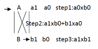
| 2x2 Vedic Multiplication algorithms: |
 |
| The general block diagram of NxN Vedic multiplier is shown in fig 5.So to implement NxN multiplier we require four ïÿýïÿý 2 ïÿýïÿý ïÿýïÿý 2 Multipliers and two N bit adders, a half adder and ïÿýïÿý 2 Bit adder. |
| We have designed a standard cell library for individual gate such as sum block, carry block, AND gate by replacing DCVS network in ECRL logic shown in fig 2 with corresponding sum block, carry block, AND gate shown fig 6. Make use of these cells, we have designed FULL adder, half adder, and a multiplier block of variable bit length using tanner tool. |
V.EXPERIMENTAL RESULTS AND COMPARISON
|
| During simulation, we have been applied 1.8V supply voltage, A= [a7, a6, a5, a4, a3, a2, a1, a0] and B= [b7, b6, b5, b4, b3, b2, b1, b0] as inputs. The pattern of inputs applied is all ones and simulation results are shown in fig 7. |
| In Fig 8,The number of transistors utilization for 2x2, 4x4 and 8x8 is reduced by 40.9%, 43.04%and 43.43%, respectively .Also Power consumption reduced by 18.2%, 55.08% and 50.66% respectively for 2x2,4x4 and 8x8 Vedic multiplier . Power consumption of both EEAL and ECRL logic shown in fig 9. |
VI. CONCLUSION
|
| A low power area efficient adiabatic structure based on the urdhava triyakbham sutra of Vedic mathematics has been proposed using ECRL logic. It can be concluded that utilization of the number of transistors has been reduced compared to the EEAL logic. Also concluded that power Consumption can be enhanced in the proposed adiabatic logic. |
| |
Figures at a glance
|
 |
 |
 |
 |
 |
| Figure 1 |
Figure 2 |
Figure 3 |
Figure 4 |
Figure 5 |
 |
 |
 |
 |
| Figure 5 |
Figure 6 |
Figure 7 |
Figure 9 |
|
| |
References
|
- M. Chanda, S. Benerjee, D. Saha, S. Jain,“Novel transistor level realization of ultra low power high speed adiabatic Vedic,” IEEE Automation, Computing, Communication, Control and Compressed Sensing (iMac4s),International Multi--Conference,kottayam,India,pp.801-806, 22-23 March 2013.
- B. Jagadguru Swami Sri Bharath, KrsnaTirathji, “Vedic Mathematics or Sixteen Simple Sutras From The Vedas”, MotilalBanarsidas,Varanasi(India), 1986.
- M.E Paramasivam and R.S Sabeenian, “An efficient bit reduction binary multiplication algorithm using Vedic methods,” IEEE 2nd International Advance Computing Conference, Patiala, India, pp. 25, 19-20 Feb. 2010.
- Richa Singh, Rajesh Mehra,”POWER EFFICIENT DESIGN OF MULTIPLEXER USING ADIABATIC LOGIC, “International Journal ofAdvances in Engineering & Technology, Vol. 6, Issue 1, pp. 246-254,Mar. 2013.
|