Research & Reviews: Journal of Engineering and Technology
ISSN: 2319-9873
ISSN: 2319-9873
Chee Kian Yap*
Department of Engineering Technologies, Queensland University of Technology, Brisbane, Australia
*Corresponding Author:
Received: 13-Mar-2024, Manuscript No. JET-24-129418; Editor assigned: 15-Mar-2024, PreQC No. JET-24-129418 (PQ); Reviewed: 19-Mar-2024, QC No. JET-24-129418; Revised: 18-Feb-2025, Manuscript No. JET-24-129418 (R); Published: 25-Feb-2025, DOI: 10.4172/2319-9873.14.1.001
Citation: Yap CK. Magnetic Step Response of 0-Dimensional 1T-CrTe2 Monolayer Nano Magnet with In-Plane Anisotropy Magnetoresistance. RRJ Eng Technol. 2025;14:001.
Copyright: © 2025 Yap CK. This is an open-access article distributed under the terms of the Creative Commons Attribution License, which permits unrestricted use, distribution and reproduction in any medium, provided the original author and source are credited.
Visit for more related articles at Research & Reviews: Journal of Engineering and Technology
Calculations show magnetic step response of larger supercell of size approximately 2 nano2 area is better perform than its smaller size cell. The calculations assumed that the in-plane Anisotropy Magnetoresistance (AMR) of the crystal is maintained down in the monolayer thickness limit. This work provides the insight that the surface area of 2D spintronics or magnetic sensors cannot be arbitrarily small for performance optimization.
AMR; Heisenberg model; Monolayer; Quantum electronics; Spintronics; Two-dimensional magnet
Since graphene was achieved in a single atomic thin layer by mechanical exfoliation in 2004, it has led to discoveries of many more 2D materials theoretically and experimentally. The remarkable properties of 2D materials offer us promising applications in electronic, optoelectronic, and spintronics. The bulk phase of these materials has a stronger bond within the in-plane while having a weaker van der Waals force holding the stack of layers forming the bulk phase. The discovery of two-dimensional magnetic materials [1,2], however it is not in equal pace with its non-magnetic counterparts, bulk magnetic materials are commonly known thousand years back, surprisingly 2D magnets are rare. This is due to Mermin-Wagner theorem that states that the continuous symmetry of spins orientation cannot be broken at a dimension less or lower than two, as continuous spins waves proliferate and destroy magnetic order. To rule out this restriction in low temperature, magnetic transition can happen with the opening of an anisotropy energy gap such as in Ising model or an energy barrier over spins orientation. Subsequently, 2D nano magnets like CrI3, Cr2Ge2Te6 are discovered and they offer new routes for the miniaturization and integration of devices in the post Moore’s era.
By fitting more electronic transistors into smaller areas in miniaturization process is promising to achieve low energy consumption and high-density logics and memory and it can scale up the performance of the chip as well. In such application, charges plays the role, in contrast, spintronics exploit the spins degrees of freedom of electrons in devices, such as in magnetoresistive devices. A natural question arises is whether smaller always means better in its performance, in this study we find that this may not be true for spintronics or nano magnetic sensors. To test the performance, we first determine the magnetic coupling parameter J by using first-principles calculations using VASP package, by solving for the parameter in total energy of two magnetic configurations, namely FM and sAFM-ABAB and in addition solving all together four magnetic configurations, namely FM, sAFM-ABAB, sAFM-AABB and AFM-Zigzag. Then a mathematical model of ferromagnetic was set up and solve for the response of magnetization of isolated orthogonal unit cell of various sizes under an external step increment magnetic field. Our calculation setting assumes the absence of MAE (Magnetic Anisotropy Energy), thus having no preferred easy axis. From the existing literature, we are aware that in monolayer, there may be an in-plane MAE. However, it does not contradict the outcome of comparing the performance in the absence of MAE.
We chose the material of 1T-CrTe2 because it was synthesized in recent years, and it was reported with having in-plane AMR (Anisotropy Magnetic Resistance). 1T-CrTe2 belongs to a class of Transition Metal Dichalcogenides (TMDs) materials in 1T phase that can be synthesized through chemical vapor deposition or mechanical exfoliation. In bulk phase or in multiple layers it is a ferromagnet with out-of-plane easy axis orientation in the minimum of 4 monolayers [3]. However, in its monolayer limit, it is a room-temperature Anti-Ferromagnet (AFM) having in-plane AMR at 0.6% at 300 K [4], the negative in AMR indicates vertical directed magnetism has a higher resistance. The AFM-Zigzag configuration of the monolayer magnet is reported to be the most stable one [5], and FM configuration has higher energy than all other two AFM configurations (sAFM-ABAB and sAFM-AABB) in the particular paper (Figures 1 and 2).

Figure 1. (a) Band structure of sAFM-ABAB magnetic state, showing overlapping of spin majority and spin minority bands forming singlet states in AFM. There is no gap near the Fermi level and the bands intersection with the Fermi level indicates a metallic electronics state. (b) Density of States of 1T-CrSe2 sAFM-ABAB.

Figure 2. Cr atom d orbitals resolved of the three bands closest to the Fermi level.
Collinear spin polarized band calculations confirming it is a metallic state AFM shown in Figure 1. The divergence or splitting of spin-up and spin-down bands preventing electrons from getting into singlet states near the Fermi level is the source of its ferromagnetism in a stable FM state. It is observed in Figure 1b that energy asymmetry between up/down channels resulted in the up d channels needing to be filled first below the Fermi level and up to at least 2 eV before down d channels can be filled above Fermi level in the conductance states, this is expected to be the origin of AFM. The Cr atom d orbitals resolved band structure in Figure 2 indicates all 5 d orbitals of Cr atoms participate in filling up the energy of the total system.
Our toy model reduces the monolayer to 0-dimensional few atoms isolated closed equilibrium system with no translational symmetry, essentially in energy wise, it becomes a quantum multi-levels system, a departure from bands description. If the AMR is maintained down to the limit in this bottom-up miniaturization assembly, the system becomes a nano tunable resistor/sensor switched by external magnetic field. The calculations proceed by first determining J magnetic exchange coupling responsible for the magnetic order, it is solved from first principles DFT+U calculations with U=3.5 eV for onsite repelling force of alpha and beta channels in Cr atom l=2 d orbitals. From first-principles calculation, we obtained the magnetic moment of Cr atom 3.544 μB. Next, we used the unit magnetic moment of magnetic Cr atoms attached to the the lattices in supercell of 3 × 3 × 1, 3 × 3 × 1, 3 × 1 × 1, and 1 × 1 × 1 of single orthogonal cell are taken into isotropy XXX Heisenberg model Hamiltonian, as the Hamiltonian is symmetric and Hermitian consisting of Pauli matrices, it is solved for the response under a step input of external magnetic field of 1 Tesla perpendicular to the direction of current in the material plane (Figure 3).

Figure 3. (a) Top view of 1T-CrTe2 monolayer crystal. Cr (Te) atoms are colored blue (gold). The orthogonal cell lattice vector a=3.66 Å, and b=6.35 Å. (b) In-plane magnetization vector and in-plane angle θ.
From first principles DFT calculations, the energy of first neighbors FM and sAFM-ABAB configurations are obtained, with E(FM(AFM))=-29.259 (-29.263) eV and by counting the pairs of magnetic interactions, they can be decomposed as follows.
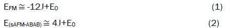
The Equations (1), (2) are formed by counting FM and AFM interactions that can be derived from Figure 4, E0 is a constant energy. Therefore, the difference in energies between FM and AFM configuration solved J to be -0.216 meV.

Figure 4. Nearest neighbors (a) FM configuration. (b) Stripe AFM-ABAB configuration. Upward arrows are Cr magnetic atoms with parallel spins and downward arrows are Cr magnetic atoms with anti-parallel spins. Red joining lines are ferromagnetic interactions and blue joining lines are anti-ferromagnetic interactions. The gray bounding box is the unit cell.
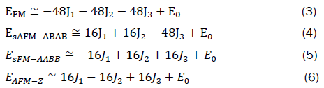
To get a more accurate J magnetic coupling parameter, we also consider up to third nearest neighbors in four magnetic configurations illustrate in Figure 5.

Figure 5. Magnetic configuration. (a) FM (b) sAFM-ABAB (c) sAFM-AABB (d) AFM-Zigzag. Red joining lines are ferromagnetic spins interaction and blue joining lines are anti-ferromagnetic interactions. The thickest line is the first nearest neighbors, followed by second and third nearest neighbors. The gray bounding box is the boundary of the unit cell.
The total energy equations are assembled as follows by counting all interactions, where J1, J2 and J3 are first, second and third nearest neighbor J coupling respectively.
The energy of various configurations and solved magnetic coupling parameter J is given in Table 1.
| Config. (U=3.5 eV) | Energy (eV) | Unknowns solved | (meV) |
| EFM | -117.768 | J1 | 0.437 |
| EsAFM-ABAB | -117.7501 | J2 | -0.148 |
| EsAFM-AABB | -118.085 | J3 | -5.025 |
| EAFM-Z | -118.067 | E0 | -117.995 |
Table 1. Magnetic configuration energies and solved unknowns.
The set of J parameters in Table 1 give rise to the sAFM-AABB ground state. This result is aligned with analysis by Zhu, et al. [6]. The energy of sAFM-AABB is close to AFM-Zigzag indicate they lies near the classification boundary of the two phases, evident from the following Figure 6.

Figure 6. Chart adapted from Zhu, et al. In relation to classification space, our result is located at the point enclosed by red circle with the lattice size of 3.66 Å and U=3.5 eV. The lattice by experiment is 3.8 Å. The star annotations are similar works done as specified in their paper.
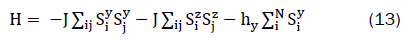
At this point, Js were determined. We continue with the description of magnetic system using isotropic XXX Heisenberg model limited by only first neighbor interactions, the Hamiltonian of the system is written as
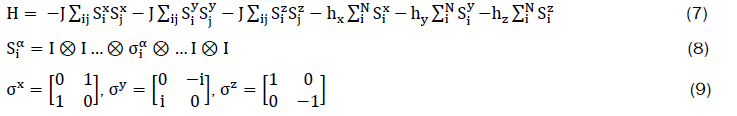
J>0 is FM exchange coupling while J<0 is AFM exchange coupling, Siα are N tensor products block with σiα are the Pauli matrices, h are external magnetic fields and I is a two dimensional identity matrix [7].
The expectation of magnetization along α is expressed below

The AMR is written as
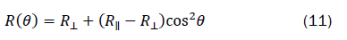
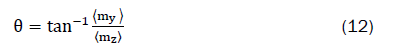
R⊥ (R||) is the resistance because of magnetization normal (parallel) to the flow of current, R⊥>R||, θ is the in-plane angle between magnetization and the x axis of the monolayer plane shown in Figure 3b. If we choose the quantization axis as x axis of the material, implies that z axis in equation (7) correspond to the x axis in material, then θ is expressed as
As only in-plane response is considered, Equation (7) can be reduced to
with z axis correspond to x axis of the material. J is set to J_1in our calculation.
The y direction of the monolayer has the highest resistance. Assume there is a magnetic field present to keep the spins oriented in the x axis as a reference position [8]. Turning off the x directed field and by applying y directed magnetic field, perpendicular to the flow of current within the material plane, the response of resistance is calculated in Figure 7.

Figure 7. The resistance of spins parallel to current is set to be zero, R||=0. The resistance of spins perpendicular to the current is set to be 1, R⊥=1 Magnetization response translated to normalized resistance by external magnetic field hy=1 Tesla of (a) 1 × 1 × 1 unit cell (b) 1 × 3 ×1 supercell (c) 3 ×1 × 1 supercell and (d) 3 × 3 × 1 supercell respectively.
It shows that all different sizes cells have a stable step response to a discrete surge of magnetic field with no overshooting or major oscillations, when stabilized the spins fully aligned along the y axis which gives maximum resistance. The smallest size cell takes the longest time to stabilize the transient to a static magnetization, which then translates into resistance value. While horizontally or vertically extended supercells, which duplicate in 3 times either in the horizontal or vertical having almost the same performance [9]. The largest cell is 3 times bigger in surface area than the single orthogonal cell exhibits the best response to magnetic field, the largest cell contains 18 Cr atoms. Thus, to get the best response for magnetic sensor, the size cannot be arbitrary small (Supplementary file).
A Heisenberg model is computed on realistic material parameters, showing 3 × 3 × 1 supercell of approximately 2 nano2 area is more stable than smaller cell, a simple intuition proven by calculation. Cells larger than the 2 nano2 are not considered due to high computational cost associated with very large dimensional vector space.
[Crossref] [Google Scholar] [PubMed]
[Crossref] [Google Scholar] [PubMed]
[Crossref] [Google Scholar] [PubMed]
[Crossref] [Google Scholar] [PubMed]
[Crossref] [Google Scholar] [PubMed]