Keywords
|
| DC–DC power conversion, soft-switching, zero-voltage-switching (ZVS). |
INTRODUCTION
|
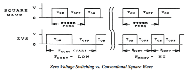
| The zero-voltage-switching (ZVS), Zero voltage switching can best be defined as conventional square wave power conversion during the switch’s on-time with switching transitions. For the most part, it can be considered as square wave power utilizing a constant off-time control which varies the conversion frequency, or on-time to maintain regulation of the output voltage. For a given unit of time, this method is similar to fixed frequency conversion which uses an adjustable duty cycle, regulation of the output voltage is accomplished by adjusting the effective duty cycle, performed by varying the conversion frequency. This changes the effective on-time in a ZVS design. The foundation of this conversion is simply the volt-second product equating of the input and output. It is virtually identical to that of square wave power conversion, and vastly unlike the energy transfer system of its electrical dual, the zero current switched converters. During the ZVS switch off-time, the L-C tank circuit resonates. This traverses the voltage across the switch from zero to its peak, and back down again to zero. At this point the switch can be reactivated, and lossless zero voltage switching facilitated. Since the output capacitance of the MOSFET switch (Co& has been discharged by the resonant tank, it does not contribute to power loss or dissipation in the switch. Therefore, the MOSFET transition losses go to zero - regardless of operating frequency and input voltage. This could represent a significant savings in power, and result in a substantial improvement in efficiency. Obviously, this attribute makes zero voltage switching a suitable candidate for high frequency, high voltage converter designs. Additionally, the gate drive requirements are somewhat reduced in a ZVS design due to the lack of the gate to drain (Miller) charge, which is deleted when V& equals zero. The technique of zero voltage switching is applicable to all switching topologies; the buck regulator and its derivatives (forward, half and full bridge), the fly back, and boost converters, to name a few. This presentation will focus on the continuous output current, buck derived topologies, converter (FBZVS converter), [1]–[5], is the most popular topology for dc–dc converters due to fixed switching frequency, ZVS operation, high efficiency, low circulating reactive energy and moderate device stresses. By using a dc blocking capacitor and a saturable inductor in series with primary winding, the primary current during the free-wheeling interval can be reduced to zero. This circuit is called as the zero-voltage and zero-current-switching (ZVZCS) FB converter [6] wherein the lagging-leg switches operate at ZCS and leading-leg switches operate with ZVS. The major limitation of the FBZVS converter has been the limited range of operation over which ZVS can be achieved. When the load current is low, the ZVS of the lagging-leg switches is lost as the energy stored in the leakage inductance of the transformer is insufficient to discharge the switch and transformer capacitances. The loss of ZVS results in increased switching losses and electromagnetic interference (EMI). In the case of high-power converters using insulated gate bipolar transistor (IGBT), an external snubber capacitor is connected to reduce the rate of rise of voltage and turn-off losses Therefore, in high-power converters, the loss of ZVS addition-ally results in the discharge of snubber capacitor in IGBT. The resulting surge current can be detrimental to IGBT and capacitor in the long run and it increases EMI problem. Further, the resonant voltage overshoots due to resonance between the snubber capacitor and wiring/lead inductance can exceed IGBT voltage rating. Therefore, it is important to maintain ZVS operation over the entire range of operation or the conversion range. The following solutions have been proposed in the past. Using higher series inductance increases the ZVS range but results in increased loss of duty cycle and ringing across secondary-side rectifier diodes. With consequent reduction in transformer turns ratio, primary reflected current and switch conduction loss increases [2], [5]. |
| 1) Using saturable inductor instead of a linear inductor, ZVS range can be increased without significantly losing the duty ratio [7], [8]. However, a large-size core is required to implement the saturable inductor. |
| 2) The energy stored in the magnetizing inductance can also be used to aid the ZVS operation. The switch current and the conduction loss is significantly increased [9]. In the converter proposed in [10] and [11], the stored energy in the magnetizing inductance of auxiliary transformer (which is independent of load) is used to extend the ZVS range. |
| 3) Using a passive auxiliary âÃâ¬Ãâ¢poleâÃâ¬Ãâ circuit, full-range ZVS operation can be achieved [12] but the fixed circulating |
| Current results in additional conduction loss. In the above listed techniques, except for (2), the range of ZVS operation can be extended at the expense of increased full-load conduction loss. Ideally, additional energy storage is not required under full-load condition since the energy stored in transformer leakage inductance is sufficient for ZVS operation. The additional stored energy is required only when the load current is less. FBZVS converters featuring this kind of adaptive energy storage using coupled inductors are reported in [13] and [14]. A passive auxiliary add-on circuit for conventional FBZVS converter using a transformer and an uncoupled inductor to achieve ZVS operation over the entire conversion range is recently proposed [15]. In this paper a new topology of FBZVS converter is proposed to achieve ZVS over entire con-version range with minimum additional conduction loss. The proposed converter does not use auxiliary coupled inductor or transformer, rather, the main power transformer is divided into two half-rated transformers and an uncoupled inductor is used to achieve ZVS over entire conversion range. It is particularly suitable in applications where the output is required to be adjustable over a wide range and load resistance and Inductance is fixed (e.g. an electromagnet power supply). The proposed converter and its operating principle are described in Sections II and III, respectively. The design considerations are discussed in Section IV. Experimental results on a 100 kHz, 500 W prototype converters are presented in Section V demonstrating full-range ZVS operation. The proposed converter is expected to exhibit higher efficiency even at part-load operation either in its low-power (e.g., up to 1–2 kW) high-frequency (300–500 kHz) application using MOSFETs or in its high-power (e.g., 5–20 kW) low-frequency (25–50 kHz) application using IGBTs. Simplified loss analysis for a high-power application of proposed FBZVS converter with IGBTs and calculations with design parameters of a 18 kW electromagnet power supply presented in Section VI, illustrate its higher part-load efficiency. |
| A.ZVS Benefits |
| Zero power âÃâ¬Ãâ¢LosslessâÃâ¬Ãâ switching transitions, Reduced EMI / RFI at transitions, No power loss due to discharging Goss, No higher peak currents, (i.e. ZCS) same as, square wave systems, High efficiency with high voltage inputs at, and any frequency Can incorporate parasitic circuit and component L & C Reduced gate drive requirements (no âÃâ¬Ãâ¢MillerâÃâ¬Ãâ effects) Short circuit tolerant |
| B.ZVS Differences |
| Variable frequency operation (in general), Higher off state voltages in single switch, unclamped topologies Relatively new technology - users must climb the earning curve Conversion frequency is inversely proportional to load current A more sophisticated control circuit may be required |
PROPOSED FBZVS CONVERTER
|
| In Fig. 1 shows the circuit diagram of the proposed FBZVS converter. Four MOSFET or IGBT switches, , four anti-parallel diodes, , and four snubber capacitors, constitute the full-bridge switching circuit. The differences between the proposed and conventional FBZVS converter are as follows. |
| a) The dc blocking capacitor of conventional converter is split into two capacitors, and , in the proposed circuit. |
| b) While the conventional converter uses a single high-frequency transformer, it is divided into two transformers and (with primary-to-secondary turns ratio of ) in the proposed circuit. |
| c) The proposed circuit has additional inductor which adaptively stores additional energy for ZVS operation when the stored energy in transformer leakage is inadequate |
| The secondary windings of the transformers are connected in series. The leakage inductances of both the transformers are shown as a lumped inductor in series with secondary windings. The diodes , , inductors , and capacitor form the output current double rectifier and filter. is the load resistance and Lo is the load inductance, where is the input dc voltage source. The current double rectifier on the secondary side in Fig. 1 can be replaced with the full-wave bridge and centre tap rectifiers if suitable. Primary and secondary connections of the transformers for alternative rectifier configurations are shown in Fig. 2. |
PRINCIPLE OF OPERATION
|
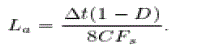
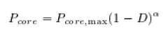
| The idealized waveforms of the converter with proposed auxiliary circuit in the steady-state are shown in Fig. 3. The details of switching transitions are not shown explicitly in the figure because the intension is to describe the operating principle of adaptive energy storage in the auxiliary inductor which aids the full-range ZVS operation and the mechanism of ZVS transitions in FB converters is well understood. Let be the duty cycle of the output voltage, , at the terminals of series-connected secondary windings of transformers and . The key waveforms for the operation when is low are shown by the solid dark lines in Fig. 3. The voltages are the gate voltage signals for switches , respectively. In steady-state the voltage across the capacitors and is equal to . The resulting voltage waveforms across the primary windings of the two transformers are shown as and . Due to the series connection of the secondary windings as shown in Fig.1, . The waveform of is a three-step bipolar square-wave voltage waveform with amplitude equal to and duty cycle . The waveform of transformer primary current is shown as and . The load current is low and the energy stored in transformer leakage inductance is not sufficient to itself achieve ZVS of all the switches . Under this condition it is desired that the sufficient energy should get stored in so that ZVS of switches can be achieved. The voltage across can be written as . The waveform of is a three-step bipolar square-wave voltage waveform with amplitude equal to and duty cycle . Therefore, when is low and load current is less, the duty cycle of is high. The peak value of is high. Sufficient energy is thus available in to achieve the ZVS operation. is derived as |
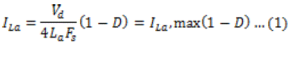 |
| Where is the switching frequency the changes in relevant waveforms for the operation of circuit when is high are shown by the dashed lines in Fig. 3. The load current is high and energy stored in the transformer leakage inductance itself is sufficient to achieve ZVS of the switches. Under this condition it is desired that the energy storage in is minimal. It is quite clear from the above discussion and from the waveforms of Fig. 3 that the duty cycle of is low. Therefore, is lower and so is the energy stored in inductor . |
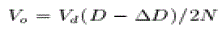
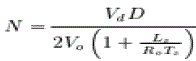
| In the applications where output is fixed (e.g. voltage regulator modules), is ideally independent of load if output filter inductor current is continuous. This continuous conduction mode (CCM) of operation is, however, practically restricted to typically up to 20% of the maximum load current otherwise the required value and size of filter inductor becomes very large In discontinuous conduction mode (DCM) D reduces with load current at No-Load condition. D≈0 In applications where the output is required to be adjustable over a wide range and load resistance and Inductance is fixed (e.g., an electromagnet power supply), the expression for load current (neglecting duty ratio loss) can be written as |
 |
| Thus, the load current and the auxiliary inductor current in the proposed circuit vary opposite to each other When is high, load current is high. Energy stored in transformer leakage inductance is sufficient for ZVS operation. Auxiliary current is low causing low additional conduction losses in the devices. When low, load is current low and energy in transformer leakage inductance is insufficient for ZVS operation. Auxiliary current increases and assists to achieve ZVS operation. Thus the trade-off between the ZVS operation and conduction losses is optimally resolved and fullrange ZVS is achieved without significantly increasing full-load conduction losses. Although the proposed FBZVS converter has two trans-formers, the combined rating of the two transformers is the same as one transformer in the conventional FBZVS converter. The primary voltage of the individual transformer in proposed converter ( , peak) is half as compared to that in conventional converter ( , peak) Thus the total volt-ampere rating of two transformer in proposed converter is the same as single transformer in conventional converter. In high-power applications two halfrated transformers in proposed converter can ease thermal management. Similarly, the worst case dc voltage That might appear across two dc blocking capacitors in the proposed converter is the same as that in the conventional FBZVS converter. |
DESIGN CONSIDERATIONS
|
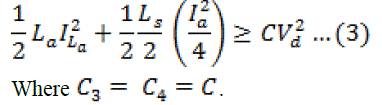
| With the same gate pulse sequence as shown in Fig. 3, in the conventional FBZVS converter, the ZVS operation of right-leg switches, and , is lost for load current lower than a certain value since energy stored in only the transformer leakage inductance (plus additional series inductor, if placed) is responsible for ZVS operation. Note that in the proposed FBZVS converter also, in absence of auxiliary inductor the ZVS operation of right-leg switches, and , is lost for lower load currents. It can be noticed from the waveforms of Fig. 3 that switches and turn-off when transformer primary current and the auxiliary inductor current are at maximum. Snubber capacitors and are charged and discharged by the total energy stored in inductors , leakage inductance of & . For higher load current, energy stored in is significant, contribution of that in the leakage inductance of is negligible and since is low; energy stored in is also insignificant. For lower load currents energy stored in still may be sufficient for ZVS operation, and in addition, ZVS of and is assisted by energy stored in as is proportionately increased. However, energy stored in is not available for ZVS operation of switches and and charging and dis-charging of and relies on energy stored in the leakage inductance of & . Under the assumption that the trans-formers and are identical having the same leakage inductance and neglecting transformer winding capacitances, the energy balance during switching transition for ZVS operation can be written as |
 |
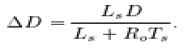
| A suitable design of approach can be to minimize the trans-former leakage inductance to minimize the duty cycle loss as well as the overshoot and ringing on the secondary side. This will also maximize the turns ratio of the transformer reducing primary-side conduction loss. The energy stored in achieves ZVS operation. From (1) and (3) |
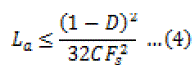 |
| However, if it is minimized, the energy stored in transformer leakage inductance may not be sufficient to achieve ZVS on its own even near full-load condition, i.e. with . Energy storage in is therefore also required even near full-load condition to achieve ZVS operation. Equation (3) gives smaller value of for 1. Smaller in turn result in large , particularly under operating conditions with 0, increasing conduction loss in the switches. Therefore, it is felt that instead of minimizing transformer leakage inductance, its value can be optimally chosen to simultaneously achieve full-range ZVS operation and improve overall efficiency over the entire conversion range. However, such an optimization is beyond the scope of this paper. |
| Additional condition can be imposed for the choice of based on time allowed to charge/discharge the |
 (5) (5) |
 (6) (6) |
 (7) (7) |
 (8) (8) |
 (9) (9) |
EXPERIMENTAL RESULTS
|
| The full-range ZVS operation in the proposed FBZVS converter is verified on an experimental 500 W prototype converter operating at 100 kHz. The converter operates from a 250 V dc input and delivers 50 A maximum in a load resistance of 0.2 , load inductance 5h. The output current variation is specified in the range of 2 to 50 A. The switches are IRF840 MOSFETs. In the trans-formers & , and . The output filter is: and . The value of auxiliary inductor is and . The control circuit was implemented with controller UC3875.The waveforms of input voltage of secondary rectifier , and for operation at various values of are shown in Fig. 4. Fig. 4(a) shows the waveforms for . As the output current is high, the energy stored in transformer leakage inductance is sufficient for ZVS operation. The duty ratio of is 0.1 and therefore is small causing minimum additional conduction loss. As progressively reduces to , as shown in Fig. 4(b), ), the duty ratio of increases to 0.5, thereby increasing . The reduced energy stored in trans-former leakage inductance is supplemented by the energy stored in in to achieve ZVS operation. As further reduces to 0.1, as shown by the waveforms of Fig. 4(c), the output current is low and the energy stored in is not sufficient for ZVS operation. However, the duty ratio of increases to 0.9 increasing and stored energy in to achieve ZVS operation The gate-source and drain-source voltage waveforms during turn-on of the left-leg switch are shown in Fig. 5(a) and (b) for and , respectively. Similarly, the gate-source and drain source voltage waveforms during turn-on of the right-leg switch are shown in Fig. 6(a) and (b) for and , respectively. Since in all the wave-forms, the gate-source voltage is applied after the drain-source voltage drops to zero, the ZVS operation of all the switches over the entire conversion range is demonstrated. Plot (1) of Fig. 7 shows the conversion efficiency of the developed prototype of the proposed converter. . Maximum conversion efficiency is limited to 0.8 primarily because the secondary-side drops become comparable with the low output voltage (10 V). The prototype converter was then reconfigured as the conventional FBZVS converter by connecting the primary windings of the two transformers in series, and connecting them between the midpoints of both the legs. To demonstrate the advantage of adaptive auxiliary current over the fixed auxiliary current, a âÃâ¬Ãâ¢poleâÃâ¬Ãâ was added to the lagging-leg of the full bridge with 120 inductor (to keep the peak circulating current same as that in the proposed converter) and capacitive voltage divider using two 1 capacitors across the input dc bus. The efficiency of conventional FBZVS converter with pole on lagging leg is shown as plot (2) in Fig. 7. From full-load to approximately 20% part-load, efficiency of the proposed converter is observed to be higher. This is because the auxiliary current in the proposed converter is lesser than that in the conventional FBZVS converter with pole on lagging leg. For lower output power, the efficiency of the proposed converter is observed to be lesser. The reason is that in the conventional FBZVS converter with pole on lagging leg, the auxiliary current is circulating in only two switches whereas in the proposed converter auxiliary current is circulating in all the four switches causing more conduction loss. A pole on leading leg is also added to conventional FBZVS converter to achieve ZVS of all the switches over the entire load range. Therefore to compare the efficiencies of proposed converter and conventional FBZVS converter with pole on both legs, another pole with 120 was added to the configured conventional FBZVS converter on the leading leg along with pole of 120 on lagging leg. The efficiency of this conventional FBZVS converter with poles on the both legs is shown as the plot (3) in Fig. 7. The efficiency is observed to be further de-graded at full-load and also over the entire range as compared to the efficiency of the proposed converter. The improvement in efficiency with the proposed converter with respect to the conventional FBZVS converter at part-load operation depends on the trade-off between switching losses saved by maintaining ZVS operation and the additional conduction loss in the switches due to circulating current plus losses in the auxiliary inductor. The savings in the switching losses which will be larger if either switching frequency is high (typically 300– 500 kHz in low-power applications, e.g., up to 1–2 kW, using MOSFET) or the snubber capacitors are larger (tens of nano farads) in high-power converters (e.g. up to 5–20 kW, using IGBT). Simplified loss analysis and calculations described in Section VI illustrates this. Nevertheless, the full-range ZVS operation achievable in the proposed converter without additional loss penalty at full-load, is the major advantage as safe operation of semiconductor devices, snubber capacitors is guaranteed and overall reliability is increased. |
SIMPLIFIED LOSS ANALYSIS OF THE PROPOSED FBZVS CONVERTER WITH IGBT SWITCHES
|
| IGBTs are used for the high-power application of proposed FBZVS converter. To calculate the conduction losses in the IGBT switches and anti-parallel diodes as well as the losses in the auxiliary inductor over the entire conversion range, following simplifying assumptions are made. |
| 1) The output current is ripple-free; therefore transformer primary current is square-wave. |
| 2) Transformer leakage inductance is small; therefore the slew interval (during which the transformer primary current reverses its direction) is absent. |
| 3) The average power loss in an IGBT and a diode is proportional to the respective average currents |
| A Device Conduction Loss |
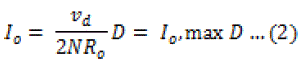
| The current flowing out of the midpoint of the leading leg is the sum of and (see Fig. 1). Similarly the current flowing out of the midpoint of lagging leg is the difference between and . The amplitude of and is equal to where is given by (2). Two distinctive modes can be observed de-pending on whether or . |
| The boundary between the two modes can be derived by equating to , The duty ratio, where the two currents have same amplitude is termed as and can be derived as |
 (10) (10) |
| Fig. 8(a) and (b) shows various current waveforms for and respectively. The expressions for average currents in all IGBT switches and antiparallel diodes of the full-bridge circuit are summarized in Table I. Expressions for the total conduction losses in these devices, , can then be derived as follows. |
| For D < Dboundry |
 |
 |
|
| For D < Dboundry |
 |
| B. Core and Winding Loss in Auxiliary Inductor |
| The core loss of ferrites is often expressed in the form of following curve-fit equation. |
 (13) (13) |
| Where , and are the constants and their values depend on the material grade. In the auxiliary inductor of the proposed converter, is constant and is proportional to , which from (1), is proportional to . Therefore, core loss in the auxiliary inductor can be expressed as |
 (14) (14) |
| where is the maximum designed core loss corresponding to . Winding loss in the auxiliary inductor are given by |
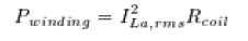 |
| where is the winding resistance and is the rms value of , given by |
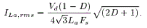 |
| C. Total Primary-Side Losses and Comparison With |
| Conventional FBZVS Converter |
| The total primary-side losses in the proposed converter are given by |
 |
| For conventional FBZVS converter, the expression for the total primary-side loss (equal to the conduction loss in IGBTs and anti-parallel diodes), can be derived as |
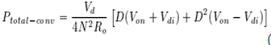 |
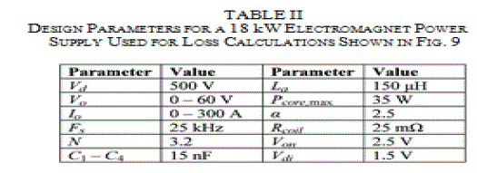
| For a 18 kW (60 V/300 A) output electromagnet power supply with designed parameters listed in Table II, Fig. 9 compares the total primary-side losses in the proposed and conventional FBZVS converter over the entire conversion range. These plots are obtained using (10)–(18) and the parameters of Table II. It can easily be seen that the total primary-side losses in the proposed converter are the same as conventional FBZVS converter for operation with higher values of (full-load operation). For the lower values of , the device conduction plus magnetics losses are higher (e.g. 111 W at 0) in the pro-posed FBZVS converter due to auxiliary circulating current. However, the loss of ZVS with 15 nF snubber capacitors in the conventional FBZVS converter would have resulted in total loss of 187.5 W. Therefore, the proposed converter improves the overall efficiency for lower values of in addition to the full-range ZVS operation. |
CONCLUSION
|
| A new FBZVS converter is proposed with ZVS of active switches over the entire conversion range. The principle of operation and design considerations of the circuit are described. The experimental results on a 500 W prototype converter demonstrate the adaptive auxiliary current which is high at lower duty ratio assisting the ZVS operation and low at higher duty ratio minimizing the additional conduction loss. The experimental results confirm the full-range ZVS operation. The proposed converter is therefore deemed suitable particularly for high-power applications where full-range ZVS operation is desired without the penalty of additional losses at full-load not only for the saving of switching losses but also for the reliable operation due to elimination of current and voltage stresses on the devices and EMI which results from the non-ZVS operation. |
 |
| Matlab SIMULATION OF A DC-AC-DC Converter with Zero-Voltage-Switching |
 |
 |
| OUTPUT OF SIMULATION |
Figures at a glance
|
 |
 |
 |
 |
| Figure 1 |
Figure 2 |
Figure 3 |
Figure 4a |
 |
 |
 |
 |
| Figure 4c |
Figure 5 |
Figure 5a |
Figure 6 |
 |
 |
 |
 |
| Figure 7 |
Figure 8 |
Figure 8a |
Figure 9 |
|
References
|
- R. A. Fischer, R. D. T. Ngo, and M. H. Kuo, âÃâ¬Ãâ¢A 500 kHz, 250Wdc–dc converter with multiple outputs controlled by phase-shifted PWM andmagnetic,âÃâ¬Ãâ in Proc. High Freq Power Conv., May 1988, pp. 100–110.
- J. A. Sabate, V. Vlatkovic, R. B. Ridley, F. C. Lee, and B. H. Cho, âÃâ¬Ãâ¢Design considerations for high-voltage high-power full-bridge zero voltageswitching PWM converter,âÃâ¬Ãâ in Proc. IEEE Appl. Power Electron. Conf. (APEC), 1990, pp. 275–284.
- D. Dalal, âÃâ¬Ãâ¢A 500 kHz multi-output converter with zero voltageSwitching,âÃâ¬Ãâ in Proc. IEEE Appl. Power Electron. Conf. (APEC), 1990, pp. 265–274.
- F.-S. Tsai, âÃâ¬Ãâ¢Small-signal and transient analysis of a zero-voltage switched, phase controlled PWM converter using averaged switch model,âÃâ¬ÃâIEEETrans. Ind. Appl., vol. 29, no. 3, pp. 493–499, May/Jun. 1993
- W. Lotfi, Q. Chen, and F. C. Lee, âÃâ¬Ãâ¢Non-linear optimization tool for the full-bridge zero-voltage-switched dc–dc convertor,âÃâ¬Ãâ Proc. Inst. Elect.Eng. B, vol. 140, no. 5, pp. 289–296, Sep. 1993.
- J. G. Cho, J. A. Sabate, G. Hua, and F. C. Lee, âÃâ¬Ãâ¢Zero-voltage and zero-current-switching full bridge PWM converter for high powerapplications,âÃâ¬ÃâIEEE Trans. Power Electron., vol. 11, no. 4, pp. 622–627,Jul. 1996.
- G. Hua, F. C. Lee, and M. M. Jovanovic, âÃâ¬Ãâ¢An improved full-bridge zero-voltage-switched PWM converter using a saturable inductor,âÃâ¬ÃâIEEETrans. Power Electron., vol. 8, no. 4, pp. 530–534, Oct. 1993.
- S. Hamada and M. Nakaoka, âÃâ¬Ãâ¢Analysis and design of a saturable reactor assisted soft-switching full-bridge dc–dc converter,âÃâ¬Ãâ IEEE Trans. PowerElectron., vol. 9, no. 3, pp. 309–317, May 1994.
- Watson and F. C. Lee, âÃâ¬Ãâ¢Analysis, design and experimental results of a 1-kW FB-ZVS-PWM converter employing magma secondary sidecontrol,âÃâ¬Ãâ IEEE Trans. Ind. Electron., vol. 45, no. 5, pp. 806–814, Oct.1998.
- R. Ayyanar and N. Mohan, âÃâ¬Ãâ¢Novel soft-switched dc–dc converter with full ZVS-range and reduced filter requirement—Part I: Regulated-outputapplications,âÃâ¬Ãâ IEEE Trans. Power. Electron. vol. 16, no.2, pp. 184–192, Mar. 2001.
- R. Ayyanar and N. Mohan, âÃâ¬Ãâ¢Novel soft-switched dc–dc converter with full ZVS-range and reduced filter requirement—Part II: Constant input,variable-output applications,âÃâ¬Ãâ IEEE Trans. Power. Electronics. vol. 16, no. 2, pp. 193–200, Mar. 2001.
- P. K. Jain, W. Kang, H. Soin, and Y. Xi, âÃâ¬Ãâ¢Analysis and design considerations of a load and line independent zero voltage switching full bridgeDC/DC converter topology,âÃâ¬Ãâ IEEE Trans. Power Electron., vol.17, no. 5, pp. 649–657, Sep. 2002.
- Y. Jang, M. M. Jovanovic, and Y. Chang, âÃâ¬Ãâ¢A new ZVS-PWM full bridge converter,âÃâ¬Ãâ IEEE Trans. Power Electron., vol. 18, no. 5, pp.1122–1129, Sep. 2003.
- Y. Jang and M. M. Jovanovic, âÃâ¬Ãâ¢A new family of full-bridge ZVS converters,âÃâ¬ÃâIEEE Trans. Power Electron., vol. 19, no. 3, pp. 701–708,May2004.
- M. Borage, S. Tiwari, and S. Kotaiah, âÃâ¬Ãâ¢A passive auxiliary circuit achieves zero-voltage-switching in full-bridge converter over entireconversion range,âÃâ¬Ãâ IEEE Power Electron. Lett., vol. 3, no. 4, pp..
- A. W. Lotfi, Q. Chen, and F. C. Lee, âÃâ¬Ãâ¢Non-linear optimization tool for the full-bridge zero-voltage-switched dc–dc convertor,âÃâ¬Ãâ Proc. Inst. Elect.Eng. B, vol. 140, no. 5, pp. 289–296, Sep. 1993.
|