Keywords
|
| step-up dc–dc converter, distributed generation system, high step-up voltage gain. |
INTRODUCTION
|
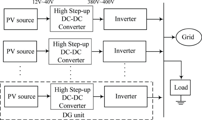
| The distributed generation (DG) systems based on the renewable energy sources have rapidly developed in recent years. These DG systems are powered by micro sources such as fuel cells, photovoltaic (PV) systems, and batteries. Fig. 1.1 shows a PV distributed system in which the solar source is low dc input voltage. |
| PV sources can also connect in series to obtain sufficient dc voltage for generating ac utility voltage; however, it is difficult to realize a series connection of the PV source without incurring a shadow effect. High step-up dc–dc converters are generally used as the frontend converters to step from low voltage (12–40 V) to high voltage (380–400 V). High step-up dc–dc converters are required to have a large conversion ratio, high efficiency, and small volume. |
| Distributed energy resource (DER) systems are small-scale power generation technologies (typically in the range of 3 kW to 10,000 kW) used to provide an alternative to or an enhancement of the traditional electric power system. The usual problems with distributed generators are their high costs. |
PROPOSED CONVERTER
|
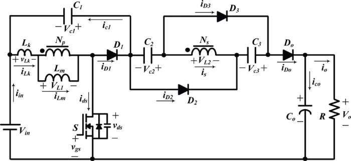
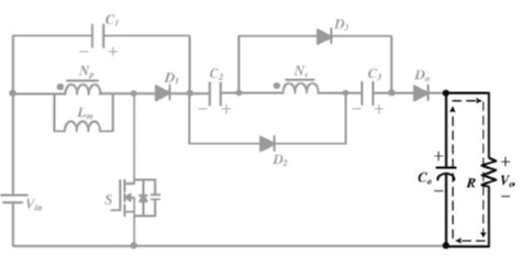
| This Proposed Converter has a high efficiency, high step-up voltage gain, and clamp-mode converter. The proposed converter adds two pairs of additional capacitors and diodes to achieve high step-up voltage gain. The coupled inductor is used as both a forward and flyback type; thus, the two capacitors can be charged in parallel and discharged in series via the coupled inductor. The transit current does not flow through the main switch compared with earlier studies. Thus, the proposed converter has low conduction loss. Additionally, this converter allows significant weight and volume reduction compared with other converters. Another benefit is that the voltage stresses on the main switch and output diode are reduced. However, the leakage inductor of the coupled inductor may cause high power loss and voltage spike. Thus, a passive clamping circuit is needed to recycle the leakage-inductor energy of the coupled inductor and to clamp the voltage across the main switch. The reverse-recovery problems in the diodes are alleviated, and thus, high efficiency can be achieved. |
Operation
|
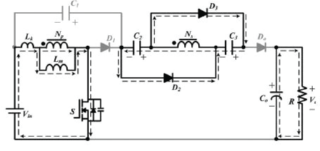
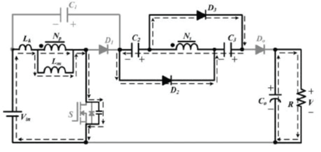
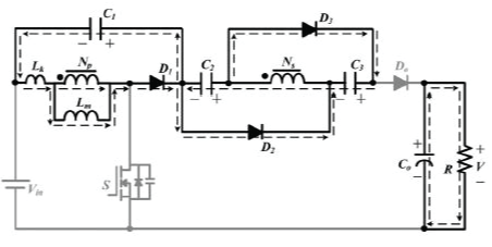
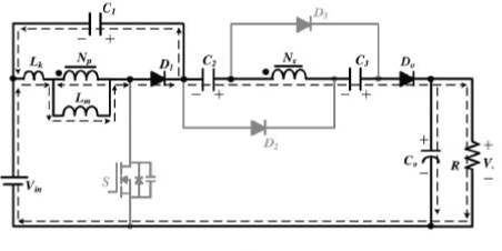
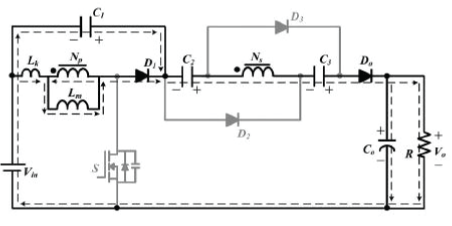
| This converter consists of dc input voltage Vin , power switch S, coupled inductors Np and Ns , one clamp diode D1, clamp capacitor C1 , two blocking capacitors C2 and C3 , two blocking diodes D2 and D3 , output diode Do , and output capacitor Co . The coupled inductor is modeled as the magnetizing inductor Lm and leakage inductor Lk . |
| To simplify the circuit analysis, the following conditions are assumed. |
| 1) Capacitors C2 , C3 , and Co are large enough that Vc2, Vc3 , and Vo are considered to be constant in one switching period. |
| 2) The power MOSFET and diodes are treated as ideal, but the parasitic capacitor of the power switch is considered. |
| 3) The coupling coefficient of coupled inductor k is equal to Lm/(Lm+Lk ) and the turns ratio of coupled inductor n is equal to Ns /Np. |
Continuous-Conduction Mode (CCM) Operation
|
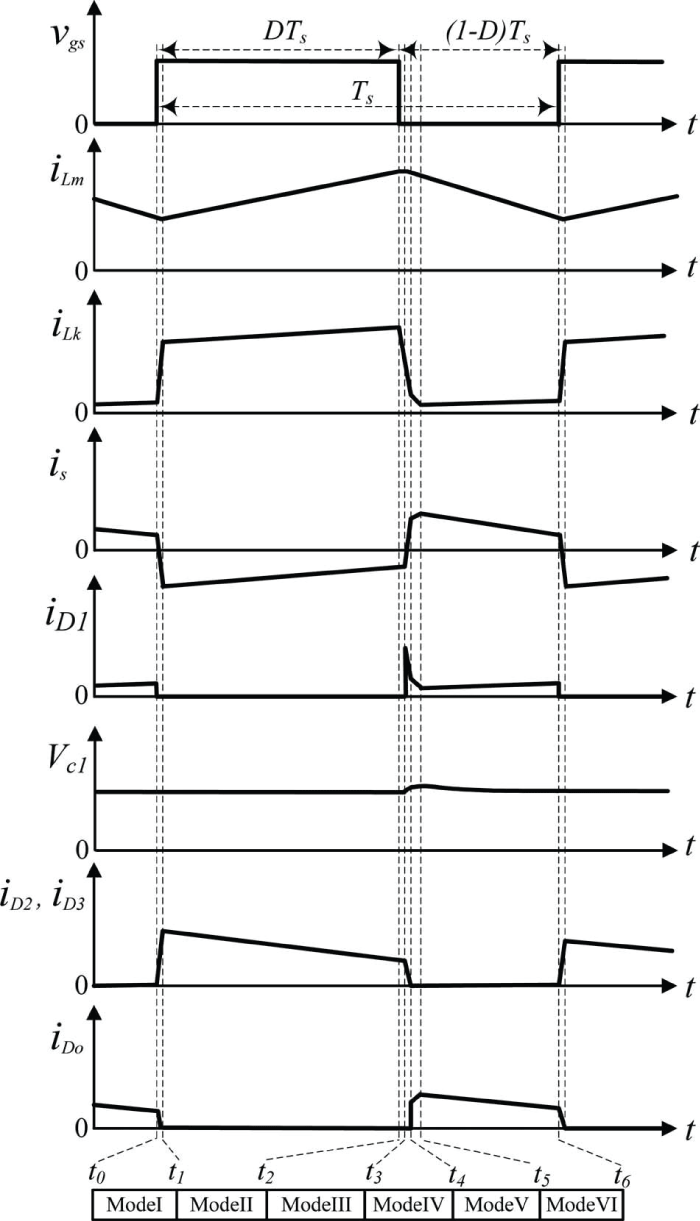
| In CCM operation, there are six operating modes in one switching period of the proposed converter. The operating modes are described as follows. |
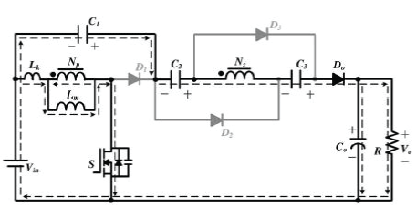
| Mode I [t0 , t1 ]: During this time interval, S is turned on. Diodes D1, D2, and D3 are turned off and Do is turned on. The current-flow path is shown in Fig.2. The primary-side current of the coupled inductor iLk is increased linearly. The magnetizing inductor Lm stores its energy from dc source Vin. Due to the leakage inductor Lk , the secondary-side current of the coupled inductor is is decreased linearly. The voltage across the secondary side winding of the coupled inductor VL 2 , and blocking voltages Vc2 and Vc3 are connected in series to charge the output capacitor Co and to provide the energy to the load R. When the current is becomes zero, dc source Vin begins to charge capacitors C2 and C3 via the coupled inductor. When iLk is equal to iLm at t = t1 , this operating mode ends. |
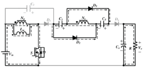
| Mode II [t1 , t2 ]: During this time interval, S is still turned on. Diodes D1 and Do are turned off, and D2 and D3 are turned on. The current-flow path is shown in Fig. 3. The magnetizing inductor Lm is stored energy from dc source Vin . Some of the energy from dc source Vin transfers to the secondary side of the coupled inductor to charge the capacitors C2 and C3. Voltages Vc2 and Vc3 are approximately equal to nVin . Output capacitor Co provides the energy to load R. This operating mode ends when switch S is turned off at t = t2 . |
| Mode III [t2 , t3 ]: During this time interval, S is turned off. Diodes D1 and Do are turned off, and D2 and D3 are turned on. The current-flow path is shown in Fig. 4. The energies of leakage inductor Lk and magnetizing inductor Lm are released to the parasitic capacitor Cds of switch S. The capacitors C2 and C3 are still charged by the dc source Vin via the coupled inductor. The output capacitor Co provides energy to load R. When the capacitor voltage Vin+Vds is equal to Vc1 at t = t3, diode D1 conducts and this operating mode ends. |
| Mode IV [t3 , t4 ]: During this time interval, S is turned off. Diodes D1 , D2 , and D3 are turned on and Do is turned off. The current-flow path is shown in Fig.5. The energies of leakage inductor Lk and magnetizing inductor Lm are released to the clamp capacitor C1 . Some of the energy stored in Lm starts to release to capacitors C2 and C3 in parallel via the coupled inductor until secondary current is equals to zero. Meanwhile, current iLk is decreased quickly. Thus, diodes D2 and D3 are cut off at t = t4 , and this operating mode ends. |
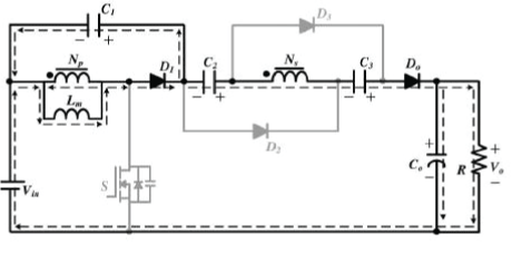
| Mode V [t4 , t5 ]: During this time interval, S is turned off. Diodes D1 and Do are turned on, and D2 and D3 are turned off. The current-flow path is shown in Fig.6. The energies of leakage inductor Lk and magnetizing inductor Lm are released to the clamp capacitor C1 . The primary and secondary windings of the coupled inductor, dc sources Vin , and capacitors C2 and C3 are in series to transfer their energies to the output capacitor Co and load R. This operating mode ends when capacitor C1 starts to discharge at t = t5 . |
| Mode VI [t5 , t6 ]: During this time interval, S is still turned off. Diodes D1 and Do are turned on, and D2 and D3 are turned off. The current-flow path is shown in Fig.7. The primary-side and secondary-side windings of the coupled inductor, dc sources Vin , and capacitors, C1 , C2 , and C3 , transfer their energies to the output capacitor Co and load R. This mode ends at t = t6 when S is turned on at the beginning of the next switching period. |
Dis-Continuous Conduction Mode (DCM) Operation
|
| In order to simplify the analysis for DCM operation, leakage inductor Lk of the coupled inductor is neglected. There are three modes in DCM operation. The operating modes are described as follows. |
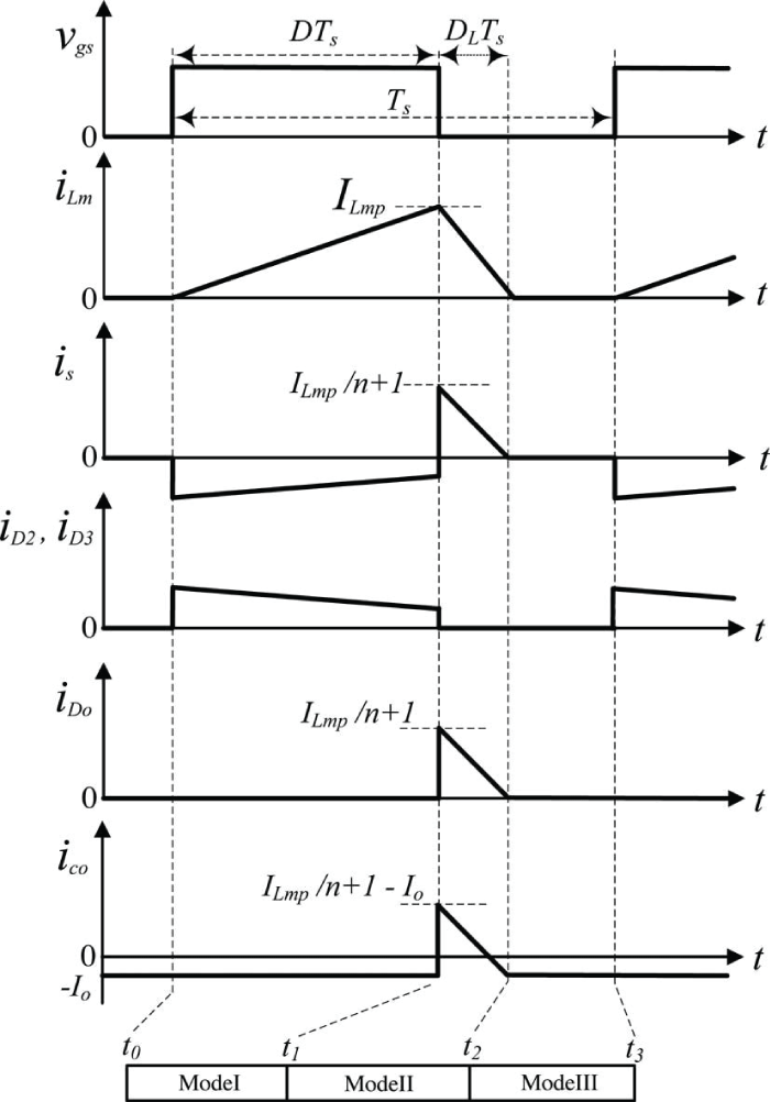
| Mode I [t0 , t1 ]: During this time interval, S is turned on. The current-flow path is shown in Fig.9.The part energy of dc source Vin transfers to magnetizing inductor Lm. Thus, iLm is increased linearly. The dc source Vin also transfers another part energy to charge capacitors C2 and C3 via the coupled inductor. The energy of the output capacitor Co is discharged to load R. This mode ends when S is turned off at t = t1 . |
| Mode II [t1 , t2 ]: During this time interval, S is turned off. The current-flow path is shown in Fig.10. The energy of the magnetizing inductor Lm is released to the capacitor C1. Similarly, capacitors C2 and C3 are discharged in a series with dc source Vin and magnetizing inductor Lm to the capacitor Co and load R. This mode ends when the energy stored in Lm is depleted at t = t2. |
| Mode III [t2 , t3 ]: During this time interval, S remains turned off. The current-flow path is shown in Fig.11. Since the energy stored in Lm is depleted, the energy stored in Co is discharged to load R. This mode ends when S is turned on at t = t3. |
STEADY STATE ANALYSIS
|
CCM Operation
|
| At modes IV and V, the energy of the leakage inductor Lk is released to the clamped capacitor C1. According to previous work, the duty cycle of the released energy can be expressed as |
 |
| Equations (11)–(13) mean that with the same specifications, the voltage stresses on the main switch and diodes can be adjusted by the turn’s ratio of the coupled inductor. |
DCM Operation
|
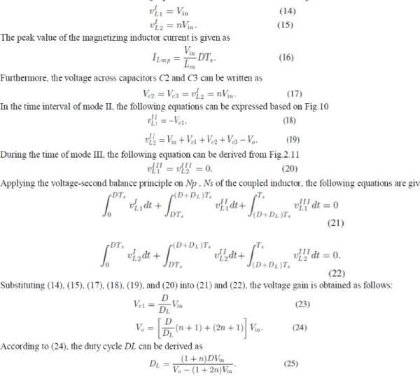
| DCM operation, three modes are discussed. The key waveform is shown in Fig. 5. During the time of mode I, the switch S is turned on. Thus, the following equations can be formulated based on Fig.9 |
 |
SIMULINK MODELS AND RESULTS
|
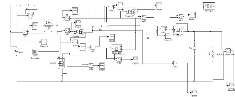
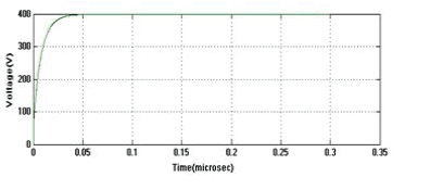
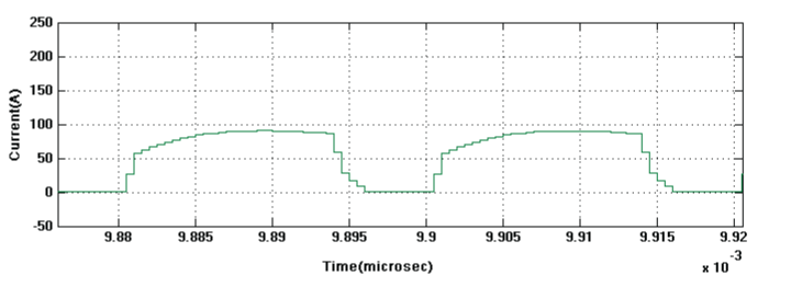
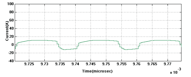
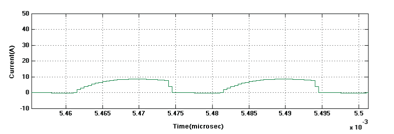
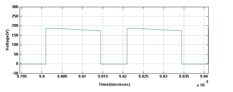
| The MATLAB/Simulink model of the proposed converter under full load condition (Po=400W) is shown in Fig.4.1. The output voltage 400v obtained is shown in Fig.4.2. The proposed converter is operated in CCM under full-load cindition.The corresponding diode voltage and current waveforms are shown in Fig’s.4.3-4.11.Fig.4.3 Output voltage waveform for proposed converter in CCM operation at Vds is clamped at appropriately 70v. Fig. 4.5 Output current waveform for proposed converter in CCM operation at IS is clamped at appropriately 10A. Fig’s.4.7&4.8 the Output current waveforms of Id2 and Id3 show that capacitors C2 and C3 are charged in parallel. The diode currentsID2and ID3 are clamped at appropriately 8A. Fig.4.10.Output current waveform for proposed converter in CCM operation at Id0 is clamped at appropriately 10A. Fig.4.11. is Output voltage waveforms for proposed converter in CCM operation at Vd0 shows the voltage stresses of the main switch and diodes. |
CONCLUSION
|
| A step-up dc–dc converter is designed and Simulated in this project. By using the capacitor charged in parallel and discharged in a series by the coupled inductor, a high step-up voltage gain is achieved. The steady-state analysis of voltage gain is discussed in detail. Simulation results confirm that high step-up voltage gain is achieved. Moreover, the proposed converter has simple structure. It is suitable for renewable energy systems in microgrid applications. |
Tables at a glance
|
 |
| Table 1 |
|
Figures at a glance
|
 |
 |
 |
 |
 |
| Figure 1 |
Figure 1a |
Figure 2 |
Figure 3 |
Figure 4 |
|
 |
 |
 |
 |
 |
| Figure 5 |
Figure 6 |
Figure 7 |
Figure 8 |
Figure 9 |
|
 |
 |
 |
 |
 |
| Figure 10 |
Figure 11 |
Figure 12 |
Figure 13 |
Figure 14 |
|
 |
 |
 |
 |
 |
| Figure 15 |
Figure 16 |
Figure 17 |
Figure 18 |
Figure 19 |
|
 |
 |
 |
 |
| Figure 20 |
Figure 21 |
Figure 22 |
Figure 23 |
|
References
|
- Y. Li and Y. W. Li, “Decoupled power control for an inverter based low voltage microgrid in autonomous operation,” in Proc. IEEE Int. PowerElectron. Motion Control Conf. (IPEMC), 2009, pp. 2490–2496.
- Y. Li, D. M. Vilathgamuwa, and P. H. Loh, “Design, analysis, and real-time testing of a controller for Multibusmicrogrid system,” IEEETrans. Power Electron., vol. 19, no. 5, pp. 1195–1204, Jul. 2004.
- C. L. Chen, Y. W, J. S. Lai, Y. S. Lee, and D. Martin, “Design of parallel inverters for smooth mode transfer microgrid applications,” IEEETrans. Power Electron., vol. 25, no. 1, pp. 6–15, Jan. 2010.
- Timbus, M. Liserre, R. Teodorescu, P. Rodriguez, and F. Blaabjerg, “Evaluation of current controllers for distributed power generationsystems,” IEEE Trans. Power Electron., vol. 24, no. 3, pp. 654–664, Mar. 2009.
- Y. A.-R. I. Mohamed and E. F. El Saadany, “Hybrid variable-structure control with evolutionary optimum-tuning algorithm for fast gridvoltageregulation using inverter-based distributed generation,” IEEE Trans. Power Electron, vol. 23, no. 3, pp. 1334–1341, May 2008.
- Y. A.-R. I. Mohamed and E. F. El Saadany, “Adaptive decentralized droop controller to preserve power sharing stability of paralleled invertersin distributed generation microgrids,” IEEE Trans. Power Electron., vol. 23, no. 6, pp. 2806–2816, Nov. 2008.
- Y. W. Li and C. -N. Kao, “An accurate power control strategy for power electronics- interfaced distributed generation units operating in a lowvoltage multibusmicrogrid,” IEEE Trans. Power Electron., vol. 24, no. 12, pp. 2977–2988, Dec. 2009.
- H. Karimi, A. Yazdani, and R. Iravani, “Negative-sequence current injection for fast islanding detection of a distributed resource unit,” IEEETrans. Power Electron., vol. 23, no. 1, pp. 298–307, Jan. 2008.
- T. Shimizu, K.Wada, andN.Nakamura, “Flyback-type single-phase utility interactive inverter with power pulsation decoupling on the dc inputfor an ac photovoltaic module system,” IEEE Trans. Power Electron, vol. 21, no. 5, pp. 1264–1272, Sep. 2006.
- L. Palma, M. H. Todorovic, and P. Enjeti, “A high gain transformer less DC–DC converter for fuel-cell applications,” in Proc. IEEE PowerElectron. Spec. Conf. (PESC), 2005, pp. 2514–2520.
|